Digital-to-Analog conversion
Question 1:
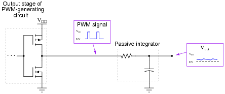
If a pulse-width modulated (PWM) signal is sent to a passive integrator circuit from a circuit capable of both sourcing and sinking current (as is the case with the dual-MOSFET output stage), the output will be a DC voltage (with some ripple):
|
|
Determine the relationship between the PWM signal's duty cycle and the DC voltage output by the integrator. What does this suggest about PWM as a means of communicating information, such as analog data from a measuring device?
Follow-up question #1: why is it important that the circuit generating the PWM signal for the integrator be able to both source and sink current?
Follow-up question #2: what would have to be done to reduce the ripple voltage at the integrator's output?
Notes:
Although it should not be difficult for students to discern the relationship between duty cycle and DC output voltage, the application of this relationship to data communication might be difficult for some students to grasp, especially on their own. Further elaboration on your part may be necessary.
An excellent example of this principle applied is the generation of an analog voltage by a 1-bit digital circuit. This technique is useful in microcontroller systems where output ports may be scarce, provided that ripple voltage (or slow response) is not a problem.
Question 2:
Explain what the purpose of a digital-to-analog converter, or DAC circuit is, in your own words.
Notes:
Informational sources abound which your students can research. Be sure to ask them to answer specifically, explaining what it means for a circuit to have a "digital input" and an änalog output."
Question 3:
Explain how this digital-to-analog converter (DAC) circuit is supposed to function:
|
|
Notes:
This question is a good review of op-amp theory, especially for students who might not have studied operational amplifiers in a while.
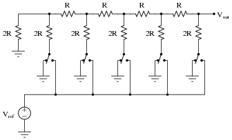
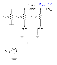
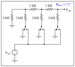
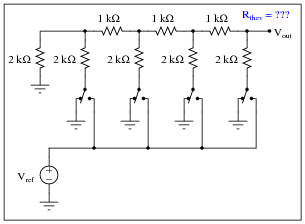
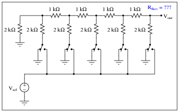
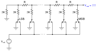
Question 4:
A type of resistor network known as an R-2R ladder is often used in digital-to-analog conversion circuits:
|
|
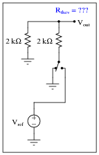
When all switches in the R-2R ladder are in the "ground" position, the network has a very interesting property regardless of its size. Analyze the Thévenin equivalent resistance (as seen from the output terminal) of the following R-2R ladder networks, then comment on the results you obtain:
|
|
|
|
|
|
|
|
|
|
Notes:
The answer is not difficult to obtain if you use each Thévenin equivalent resistance to model the left-hand portion of each successive R-2R ladder network as they become more complex! Those students who do not take this problem-solving step are doomed to perform a lot of series-parallel calculations!
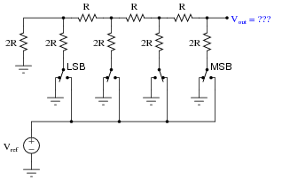
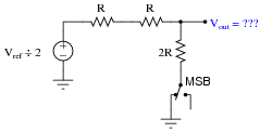
Question 5:
When only the most significant bit (MSB) of an R-2R ladder resistor network is activated (all other bits inactive, their switches connecting to ground), the output voltage will be the same, regardless of how many bits the network has:
|
|
Explain why this output voltage magnitude stands independent of the number of bits (sections) in the R-2R ladder network.
|
Notes:
The key to understanding the answer is to apply Thévenin's theorem to the ïnactive" sections of the network. Here, the unique property of constant output impedance for an R-2R network yields a useful feature when applied to DAC circuitry.
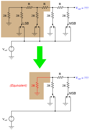
Question 6:
Thévenin's theorem is a powerful tool for analyzing R-2R ladder networks. Take for instance this four-section network where the next-to-most-significant "bit" is activated, while all the other "bits" are inactive (switched to ground):
|
|
If we Thévenize all sections to the left of the activated section, replacing it with a single resistance to ground, we see the network becomes far simpler:
|
|
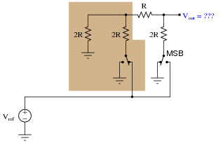
Explain how we may apply Thévenin's theorem once again to the shaded section of this next circuit (simplified from the previous circuit shown above) to simplify it even more, obtaining a final result for Vout:
|
|
|
|
Notes:
Students might not realize it is valid to iteratively apply Thévenin's theorem to the solution of a circuit problem. You can, and this stands as a good example of how (and why!) you should do it.
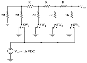
Question 7:
Determine the voltage output by the following R-2R ladder network given the switch states shown in the table:
|
|
-
SW0 SW1 SW2 SW3 Vout
Ground Ground Ground Vref
Ground Ground Vref Ground
Ground Vref Ground Ground
Vref Ground Ground Ground
Ground Ground Ground Ground
-
SW0 SW1 SW2 SW3 Vout
Ground Ground Ground Vref 8 volts
Ground Ground Vref Ground 4 volts
Ground Vref Ground Ground 2 volts
Vref Ground Ground Ground 1 volt
Ground Ground Ground Ground 0 volts
Follow-up question: the fact that an R-2R resistor network is inherently linear, we may readily apply the Superposition Theorem to figure out what happens when more than one switch is moved to the Vref position. Explain how you would apply Superposition to determine all output voltages for all possible combinations of switch positions.
Notes:
As you can see, the reference voltage value of 16 volts was not chosen at random! I wanted students to see the pattern between single switch closures and binary place-weights for a four-bit number. The actual electrical analyses for each condition are best expedited by applying Thévenin's theorem repeated to the circuit, condensing sections to single resistances and voltage sources until a simple voltage divider circuit is obtained at the output terminal.
The follow-up question is quite important. Be sure to ask your students about it, for it holds the key to figuring out all output voltage values for all binary input possibilities.
Question 8:
Explain why DAC circuits based on R-2R ladder networks are more popular than binary-weighed resistor networks. Either one will work well if properly designed and built, so why would one design be more widely manufactured?
Notes:
It is important for your students to grasp basic principles and practices of business, because that is the arena their technical skills will most likely find challenge and value. This question is a way to get your students thinking about real-life, practical manufacturing concerns that go beyond basic principles of electrical theory.
Question 9:
Explain what a digital potentiometer is, and give one example of a digital potentiometer in integrated-circuit (IC) form.
Follow-up question: would you classify a digital potentiometer as an ADC (analog-to-digital converter) or as a DAC (digital-to-analog converter)?
Notes:
Rarely is the digital potentiometer mentioned in introductory textbooks as a digital-to-analog converter device, but it is!
Question 10:
What is meant by the word resolution in reference to an ADC or a DAC? Why is resolution important to us, and how may it be calculated for any particular circuit knowing the number of binary bits?
Notes:
Note that I did not hint how to calculate the resolution of a DAC or an ADC, I just gave the answer for a particular example. The goal here is for students to inductively "work backwards" from my example to a general mathematical statement about resolution.
There are actually two different ways to calculate the resolution, depending on the actual range of the converter circuit. For the answer given, I assumed that a digital value of 0x00 = 0.00 volts DC and that a digital value of 0xFF = 10.00 volts DC. If a student were to calculate the resolution for a circuit where 0xFF generated an output voltage just shy of 10.00 volts DC (e.g. an R-2R ladder network where Vref = 10 volts DC, and a full-scale binary input generates an output voltage just one step less than Vref), the correct answer for resolution would be 39.06 mV.
You may want to bring up such practical examples of resolution as the difference between a handheld digital multimeter and a lab-bench digital multimeter. The number of digits on the display is a sure clue to a substantial difference in ADC resolution.
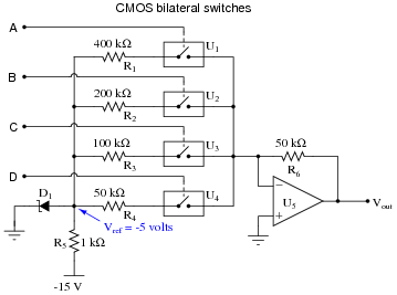
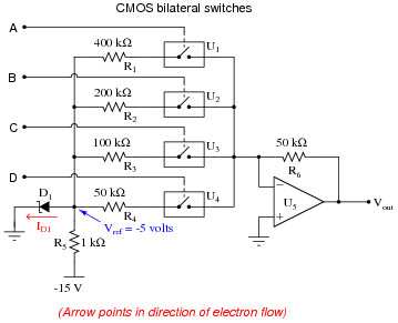
Question 11:
This digital-to-analog converter (DAC) circuit takes a four-bit binary input (input terminals A through D) and converts it to an analog voltage (Vout). Predict how the operation of this circuit will be affected as a result of the following faults. Consider each fault independently (i.e. one at a time, no multiple faults):
|
|
- �
- Bilateral switch U1 fails open:
- �
- Zener diode fails shorted:
- �
- Solder bridge (short) past resistor R1:
- �
- Resistor R6 fails open:
- �
- Bilateral switch U1 fails open: Vout same for all odd numbered input conditions as it is for next lowest even-numbered input condition (e.g. input value of 5 gives same output as input value of 4).
- �
- Zener diode fails shorted: Vout is nearly zero volts for any input condition.
- �
- Solder bridge (short) past resistor R1: Vout saturates positive for any given odd-valued input condition.
- �
- Resistor R6 fails open: Vout always saturated.
Follow-up question #1: is the arrow showing zener diode current drawn in the direction of electron flow or conventional flow?
Follow-up question #2: which input bit is the most significant (MSB) and which is the least significant (LSB)?
Notes:
Questions like this help students hone their troubleshooting skills by forcing them to think through the consequences of each possibility. This is an essential step in troubleshooting, and it requires a firm understanding of circuit function.
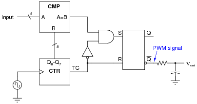
Question 12:
The following circuit generates an analog output voltage proportional to the value of the binary input, using pulse-width modulation (PWM) as an interim format. An eight-bit binary counter (CTR) continually counts in the üp" direction, while an 8-bit magnitude comparator (CMP) checks when the 8-bit binary input value matches the counter's output value. The AND gate and inverter simply prevent the S-R latch from being ßet" and "reset" simultaneously (when both A and B are maximum, both at a hex value of $FF), which would cause the output to be ïnvalid" when S and R were both active, and unpredictable when both S and R inputs returned to their inactive states:
|
|
Explain how this circuit works, using timing diagrams if necessary to help show the PWM signal at [`Q] for different input values.
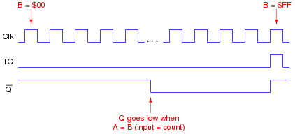
|
|
I'll leave it to you to explain the relationship between the input value (A), the PWM duty cycle, and the analog output voltage.
Notes:
This circuit provides students with an interesting exercise in timing analysis, as well as being a simple means of converting large binary values into analog output voltages without resorting to using large resistor networks.
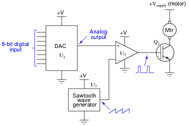
Question 13:
This is a digitally-set motor speed controller circuit, using PWM to modulate power to the motor. Predict how the operation of this circuit will be affected as a result of the following faults. Consider each fault independently (i.e. one at a time, no multiple faults):
|
|
- �
- DAC output fails low (output = 0 volts DC):
- �
- DAC output fails high (output = +V):
- �
- IGBT Q1 fails open (collector to emitter):
- �
- Solder bridge (short) between MSB input on U1 and ground:
- �
- DAC output fails low (output = 0 volts DC): Motor will not run.
- �
- DAC output fails high (output = +V): Motor runs full speed all the time.
- �
- IGBT Q1 fails open (collector to emitter): Motor will not run.
- �
- Solder bridge (short) between MSB input on U1 and ground: Speeds 0 through 127 work normally, but speeds 128 through 255 just duplicate speeds 0 through 127, respectively.
Notes:
Questions like this help students hone their troubleshooting skills by forcing them to think through the consequences of each possibility. This is an essential step in troubleshooting, and it requires a firm understanding of circuit function.