Special diodes
Question 1:
| Don't just sit there! Build something!! |
Learning to mathematically analyze circuits requires much study and practice. Typically, students practice by working through lots of sample problems and checking their answers against those provided by the textbook or the instructor. While this is good, there is a much better way.
You will learn much more by actually building and analyzing real circuits, letting your test equipment provide the änswers" instead of a book or another person. For successful circuit-building exercises, follow these steps:
- 1.
- Carefully measure and record all component values prior to circuit construction, choosing resistor values high enough to make damage to any active components unlikely.
- 2.
- Draw the schematic diagram for the circuit to be analyzed.
- 3.
- Carefully build this circuit on a breadboard or other convenient medium.
- 4.
- Check the accuracy of the circuit's construction, following each wire to each connection point, and verifying these elements one-by-one on the diagram.
- 5.
- Mathematically analyze the circuit, solving for all voltage and current values.
- 6.
- Carefully measure all voltages and currents, to verify the accuracy of your analysis.
- 7.
- If there are any substantial errors (greater than a few percent), carefully check your circuit's construction against the diagram, then carefully re-calculate the values and re-measure.
When students are first learning about semiconductor devices, and are most likely to damage them by making improper connections in their circuits, I recommend they experiment with large, high-wattage components (1N4001 rectifying diodes, TO-220 or TO-3 case power transistors, etc.), and using dry-cell battery power sources rather than a benchtop power supply. This decreases the likelihood of component damage.
As usual, avoid very high and very low resistor values, to avoid measurement errors caused by meter "loading" (on the high end) and to avoid transistor burnout (on the low end). I recommend resistors between 1 kW and 100 kW.
One way you can save time and reduce the possibility of error is to begin with a very simple circuit and incrementally add components to increase its complexity after each analysis, rather than building a whole new circuit for each practice problem. Another time-saving technique is to re-use the same components in a variety of different circuit configurations. This way, you won't have to measure any component's value more than once.
Notes:
It has been my experience that students require much practice with circuit analysis to become proficient. To this end, instructors usually provide their students with lots of practice problems to work through, and provide answers for students to check their work against. While this approach makes students proficient in circuit theory, it fails to fully educate them.
Students don't just need mathematical practice. They also need real, hands-on practice building circuits and using test equipment. So, I suggest the following alternative approach: students should build their own "practice problems" with real components, and try to mathematically predict the various voltage and current values. This way, the mathematical theory "comes alive," and students gain practical proficiency they wouldn't gain merely by solving equations.
Another reason for following this method of practice is to teach students scientific method: the process of testing a hypothesis (in this case, mathematical predictions) by performing a real experiment. Students will also develop real troubleshooting skills as they occasionally make circuit construction errors.
Spend a few moments of time with your class to review some of the "rules" for building circuits before they begin. Discuss these issues with your students in the same Socratic manner you would normally discuss the worksheet questions, rather than simply telling them what they should and should not do. I never cease to be amazed at how poorly students grasp instructions when presented in a typical lecture (instructor monologue) format!
A note to those instructors who may complain about the "wasted" time required to have students build real circuits instead of just mathematically analyzing theoretical circuits:
What is the purpose of students taking your course?
If your students will be working with real circuits, then they should learn on real circuits whenever possible. If your goal is to educate theoretical physicists, then stick with abstract analysis, by all means! But most of us plan for our students to do something in the real world with the education we give them. The "wasted" time spent building real circuits will pay huge dividends when it comes time for them to apply their knowledge to practical problems.
Furthermore, having students build their own practice problems teaches them how to perform primary research, thus empowering them to continue their electrical/electronics education autonomously.
In most sciences, realistic experiments are much more difficult and expensive to set up than electrical circuits. Nuclear physics, biology, geology, and chemistry professors would just love to be able to have their students apply advanced mathematics to real experiments posing no safety hazard and costing less than a textbook. They can't, but you can. Exploit the convenience inherent to your science, and get those students of yours practicing their math on lots of real circuits!
Question 2:
The characteristically colored glow from a gas-discharge electric light is the result of energy emitted by electrons in the gas atoms as they fall from high-level ëxcited" states back to their natural ("ground") states. As a general rule of electron behavior, they must absorb energy from an external source to leap into a higher level, and they release that energy upon returning to their original level.
Given the existence of this phenomenon, what do you suspect might be occurring inside a PN junction as it conducts an electric current?
Follow-up question: what practical application can you think of for this phenomenon?
Notes:
The practical application of this phenomenon should be obvious, and it is very commonplace in modern electronic equipment. Discuss with your students the energy-efficiency of this light emission as compared to an incandescent lamp.
Question 3:
Explain the operating principle of a photovoltaic cell, otherwise known as a ßolar cell." What happens within these devices to convert sunlight directly into electricity?
Challenge question: of what significance is the band gap of the PN junction to the efficiency of the cell?
Notes:
There is quite a bit of detail that could be added to the account given in the answer. Ask your students to supply some of this detail! There are many resources for learning how photovoltaic cells work, so your students should have no trouble finding the information on their own.
Question 4:
The nonconducting depletion region of a PN junction forms a parasitic capacitance between the P and the N semiconductor region. Does the capacitance increase or decrease as a greater reverse-bias voltage is applied to the PN junction? Explain your answer.
Challenge question: can you think of any practical applications for this variable-capacitance effect?
Notes:
This question is a good review of capacitor theory, and also an opportunity to introduce a special kind of diode: the varactor.
Question 5:
Explain what a Schottky diode is, and how it differs in construction and in function from a normal semiconductor PN junction diode.
Notes:
Ask your students if they happened to research any datasheets for Schottky diodes, and if they have parameters to compare against typical PN junction rectifying diodes such as the 1N400x series.
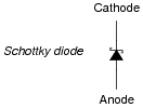
Question 6:
Draw the schematic symbol for a Schottky diode, and give some examples of typical applications for it.
|
|
I'll let you research some of the typical applications of Schottky diodes.
Notes:
Ask your students to explain why the applications of Schottky diodes are well suited for these diodes' unique capabilities. What is it about the typical applications that make use of these diodes' fast reverse-recovery times and/or low forward voltage drop?
Note to your students that the schematic symbol for a Schottky diode is easily confused with the schematic symbol for a zener diode. Pay close attention to the symbol!
Question 7:
There is a special type of diode called a varactor, which is used to create a voltage-dependent capacitance. This function is often used in electronic radio tuner circuits:

|
|
The voltage-dependent capacitance of this diode is given by the following equation:
|
Where,
CJ = Junction capacitance
Co = Junction capacitance with no applied voltage
V = Applied reverse junction voltage
Based on this equation, would you say that capacitance is directly or inversely related to the applied reverse-bias voltage of a varactor diode? Based on what you know of diode theory, explain why this makes sense.
Follow-up question: substitute the varactor diode capacitance equation into the standard resonant frequency equation to arrive at one equation solving for frequency in terms of L and diode voltage V.
Notes:
This question reinforces students' understanding of the mathematical terms direct and inverse, as well as review basic PN junction theory and capacitor theory.
Question 8:
What type of diode is always packaged in a clear glass or plastic body (as opposed to an opaque plastic body)? Explain how the appearance of the component is helpful in determining its identity.
Follow-up question: the physical size of a component is often an indication of what performance parameter?
Notes:
I usually do not ask "trick" questions such as this, but occasionally they work really well to get the point across.