Flip-flop circuits
Question 1:
| Don't just sit there! Build something!! |
Learning to analyze digital circuits requires much study and practice. Typically, students practice by working through lots of sample problems and checking their answers against those provided by the textbook or the instructor. While this is good, there is a much better way.
You will learn much more by actually building and analyzing real circuits, letting your test equipment provide the änswers" instead of a book or another person. For successful circuit-building exercises, follow these steps:
- 1.
- Draw the schematic diagram for the digital circuit to be analyzed.
- 2.
- Carefully build this circuit on a breadboard or other convenient medium.
- 3.
- Check the accuracy of the circuit's construction, following each wire to each connection point, and verifying these elements one-by-one on the diagram.
- 4.
- Analyze the circuit, determining all output logic states for given input conditions.
- 5.
- Carefully measure those logic states, to verify the accuracy of your analysis.
- 6.
- If there are any errors, carefully check your circuit's construction against the diagram, then carefully re-analyze the circuit and re-measure.
Always be sure that the power supply voltage levels are within specification for the logic circuits you plan to use. If TTL, the power supply must be a 5-volt regulated supply, adjusted to a value as close to 5.0 volts DC as possible.
One way you can save time and reduce the possibility of error is to begin with a very simple circuit and incrementally add components to increase its complexity after each analysis, rather than building a whole new circuit for each practice problem. Another time-saving technique is to re-use the same components in a variety of different circuit configurations. This way, you won't have to measure any component's value more than once.
Notes:
It has been my experience that students require much practice with circuit analysis to become proficient. To this end, instructors usually provide their students with lots of practice problems to work through, and provide answers for students to check their work against. While this approach makes students proficient in circuit theory, it fails to fully educate them.
Students don't just need mathematical practice. They also need real, hands-on practice building circuits and using test equipment. So, I suggest the following alternative approach: students should build their own "practice problems" with real components, and try to predict the various logic states. This way, the digital theory "comes alive," and students gain practical proficiency they wouldn't gain merely by solving Boolean equations or simplifying Karnaugh maps.
Another reason for following this method of practice is to teach students scientific method: the process of testing a hypothesis (in this case, logic state predictions) by performing a real experiment. Students will also develop real troubleshooting skills as they occasionally make circuit construction errors.
Spend a few moments of time with your class to review some of the "rules" for building circuits before they begin. Discuss these issues with your students in the same Socratic manner you would normally discuss the worksheet questions, rather than simply telling them what they should and should not do. I never cease to be amazed at how poorly students grasp instructions when presented in a typical lecture (instructor monologue) format!
I highly recommend CMOS logic circuitry for at-home experiments, where students may not have access to a 5-volt regulated power supply. Modern CMOS circuitry is far more rugged with regard to static discharge than the first CMOS circuits, so fears of students harming these devices by not having a "proper" laboratory set up at home are largely unfounded.
A note to those instructors who may complain about the "wasted" time required to have students build real circuits instead of just mathematically analyzing theoretical circuits:
What is the purpose of students taking your course?
If your students will be working with real circuits, then they should learn on real circuits whenever possible. If your goal is to educate theoretical physicists, then stick with abstract analysis, by all means! But most of us plan for our students to do something in the real world with the education we give them. The "wasted" time spent building real circuits will pay huge dividends when it comes time for them to apply their knowledge to practical problems.
Furthermore, having students build their own practice problems teaches them how to perform primary research, thus empowering them to continue their electrical/electronics education autonomously.
In most sciences, realistic experiments are much more difficult and expensive to set up than electrical circuits. Nuclear physics, biology, geology, and chemistry professors would just love to be able to have their students apply advanced mathematics to real experiments posing no safety hazard and costing less than a textbook. They can't, but you can. Exploit the convenience inherent to your science, and get those students of yours practicing their math on lots of real circuits!
Question 2:
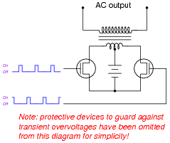
A common topology for DC-AC power converter circuits uses a pair of transistors to switch DC current through the center-tapped winding of a step-up transformer, like this:
|
|
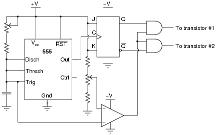
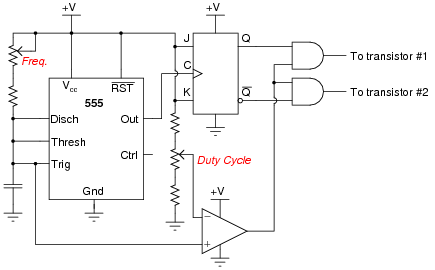
In order for this form of circuit to function properly, the transistor "firing" signals must be precisely synchronized to ensure the two are never turned on simultaneously. The following schematic diagram shows a circuit to generate the necessary signals:
|
|
Explain how this circuit works, and identify the locations of the frequency control and pulse duty-cycle control potentiometers.
|
|
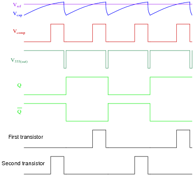
- �
- Vref = DC reference voltage set by duty cycle potentiometer
- �
- Vcap = Voltage measured at top terminal of the 555's capacitor
- �
- Vcomp = Comparator output voltage
- �
- V555(out) = 555 timer output voltage
- �
- Q = Noninverted output of J-K flip-flop
- �
- [`Q] = Inverted output of J-K flip-flop
|
|
Follow-up question: which direction would you have to move the frequency potentiometer to increase the output frequency of this circuit? Which direction would you have to move the duty cycle potentiometer to increase that as well?
Challenge question: suppose you were prototyping this circuit without the benefit of an oscilloscope. How could you test the circuit to ensure the final output pulses to the transistors are never simultaneously in the "high" logic state? Assume you had a parts assortment complete with light-emitting diodes and other passive components.
Notes:
This question is an exercise in schematic diagram and timing diagram interpretation. By the way, I have built and tested this circuit and I can say it works very well.
Question 3:
A common type of rotary encoder is one built to produce a quadrature output:
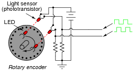
|
|
The two LED/phototransistor pairs are arranged in such a way that their pulse outputs are always 90o out of phase with each other. Quadrature output encoders are useful because they allow us to determine direction of motion as well as incremental position.
Building a quadrature direction detector circuit is easy, if you use a D-type flip-flop:
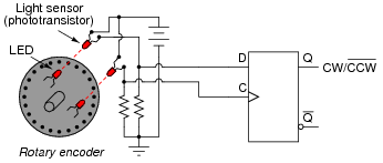
|
|
Analyze this circuit, and explain how it works.
Follow-up question: comment on the notation used for this circuit's output. What does the label "CW /[`CCW]" tell you, without having to analyze the circuit at all?
Notes:
Quadrature direction-detection circuits such as this become important when encoders are linked to digital counter circuits. The complemented notation is also very common in counter circuits.
Students may show a reluctance to draw a timing diagram when they approach this problem, even when they realize the utility of such a diagram. Instead, many will try to figure the circuit out just by looking at it. Note the emphasis on the word "try." This circuit is much more difficult to figure out without a timing diagram! Withhold your explanation of this circuit until each student shows you a timing diagram for it. Emphasize the fact that this step, although it consumes a bit of time, is actually a time-saver in the end.
Question 4:
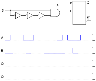
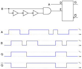
Determine the final output states over time for the following circuit, built from D-type gated latches:
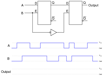
|
|
At what specific times in the pulse diagram does the final output assume the input's state? How does this behavior differ from the normal response of a D-type latch?
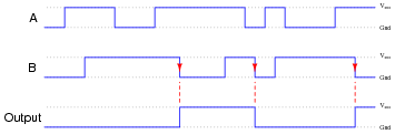
|
|
The final output assumes the same logic state as the input only when the enable input signal (B) transitions from "high" to "low".
Notes:
Note that by adding another latch, the overall behavior only slightly resembles the behavior of a D-type latch. With the addition of the second latch, we've changed this circuit into a flip-flop, specifically of the master-slave variety.
Question 5:
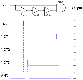
Usually, propagation delay is considered an undesirable characteristic of logic gates, which we simply have to live with. Other times, it is a useful, even necessary, trait. Take for example this circuit:
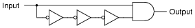
|
|
If the gates constituting this circuit had zero propagation delay, it would perform no useful function at all. To verify this sad fact, analyze its steady-state response to a "low" input signal, then to a "high" input signal. What state is the AND gate's output always in?
Now, consider propagation delay in your analysis by completing a timing diagram for each gate's output, as the input signal transitions from low to high, then from high to low:
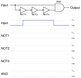
|
|
What do you notice about the state of the AND gate's output now?
|
|
Follow-up question: describe exactly what conditions are necessary to obtain a "high" signal from the output of this circuit, and what determines the duration of this "high" pulse.
Notes:
Tell your students that this circuit is a special type of one-shot, outputting a single pulse of limited duration for each leading-edge transition of the input signal.
Ask your students what we might do if we wanted to make the output pulse of this one-shot circuit longer (or shorter).
Question 6:
Explain how you would use an oscilloscope to measure the propagation delay of a semiconductor logic gate. Draw a schematic diagram, if necessary. Are the propagation delay times typically equal for a digital gate transitioning from "low" to "high", versus from "high" to "low"? Consult datasheets to substantiate your answer.
Also, comment on whether or not electromechanical relays have an equivalent parameter to propagation delay. If so, how do you suppose the magnitude of a relay's delay compares to that of a semiconductor gate, and why?
And yes, electromechanical relays also have intrinsic delay times, which tend to be far greater than those encountered with semiconductor logic gates.
Notes:
This question makes an excellent in-class demonstration. It shows this practical parameter in terms the students should be able to kinesthetically relate to.
Hold your students accountable for researching datasheets, rather than just looking up the information in a textbook. Ultimately, reading datasheets and applications notes written by the manufacturers will keep them abreast of the latest technology much more effectively than textbooks, since most textbooks I've seen tend to lag behind state-of-the-art by a few years at the least. There is wealth of information to be gained from manufacturers' literature, so prepare your students to use it!
Explain to your students that relays not only have actuation delay, but most of them also exhibit significant contact bounce as well. Contact bounce is a problem especially where relays send signals to solid-state logic circuitry, to a much greater extent than where relays send signals to other relays. Special-purpose relays can be obtained whose designs minimize actuation time and bounce, but both characteristics are far worse than any equivalent effects in semiconductor logic gates.
Question 7:
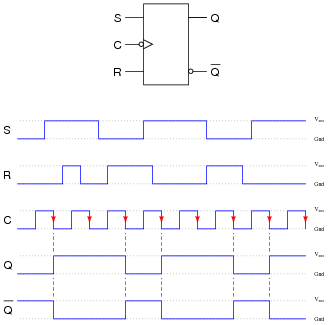
Determine the Q and [`Q] output states of this D-type gated latch, given the following input conditions:
|
|
Now, suppose we add a propagation-delay-based one-shot circuit to the Enable line of this D-type gated latch. Re-analyze the output of the circuit, given the same input conditions:
|
|
Comment on the differences between these two circuits' responses, especially with reference to the enabling input signal (B).
|
|
|
|
Follow-up question: one of these circuits is referred to as edge-triggered. Which one is it?
Challenge question: in reality, the output waveforms for both these scenarios will be shifted slightly due to propagation delays within the constituent gates. Re-draw the true outputs, accounting for these delays.
Notes:
Discuss with your students the concept of edge-triggering, and how it is implemented in (one of) the circuits in this question. Ask them to describe any tips they may have discovered for analyzing pulse waveforms. Specifically, are there any particular times where we need to pay close attention to the D input signal to determine what the outputs do, and any times where we can ignore the D input status?
The challenge question regarding propagation delays is meant to remind students that the perfectly synchronized timing diagrams seen in textbooks are not exactly what happens in real life. Ask your students to elaborate on what real-life conditions would make such propagation delays relevant. Are there applications of digital circuits where we can all but ignore such delays?
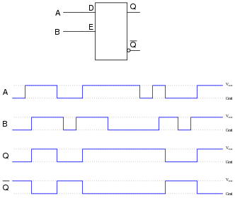
Question 8:
Shown here are two digital components: a D-type latch and a D-type flip-flop:
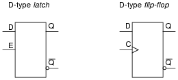
|
|
Other than the silly name, what distinguishes a "flip-flop" from a latch? How do the two circuits differ in function?
Notes:
Note to your students that the timing input of a flip-flop is called a clock rather than an enable. Ask them to identify what differences in symbolism show this distinction between the two devices.
Question 9:
Explain how the addition of a propagation-delay-based one-shot circuit to the enable input of an S-R latch changes its behavior:
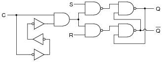
|
|
Specifically, reference your answer to a truth table for this circuit.
|
|
Challenge question: what exactly happens in the ïnvalid" state for this S-R flip-flop?
Notes:
Discuss with your students what happens in this circuit when the clock signal is doing anything other than transitioning from low to high. What condition(s) are equivalent in a regular S-R gated latch circuit?
The challenge question is especially tricky to answer. Ïnvalid" states are easy to determine in regular S-R latch circuits, gated or ungated. However, because an S-R flip-flop is only momentarily "gated" by the edge of the clock signal, the states its outputs fall to after that edge event has passed is much more difficult to determine.
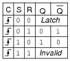
Question 10:
Plain S-R latch circuits are ßet" by activating the S input and de-activating the R input. Conversely, they are "reset" by activating the R input and de-activating the S input. Gated latches and flip-flops, however, are a little more complex:
|
|
Describe what input conditions have to be present to force each of these multivibrator circuits to set and to reset.
For the S-R gated latch:
- �
- Set by . . .
- �
- Reset by . . .
For the S-R flip-flop:
- �
- Set by . . .
- �
- Reset by . . .
- �
- Set by making S high, R low, and E high.
- �
- Reset by making R high, S low, and E high.
For the S-R flip-flop:
- �
- Set by making S high, R low, and C transition from low to high.
- �
- Reset by making R high, S low, and C transition from low to high.
Notes:
The purpose of this question is to review the definitions of ßet" and "reset," as well as to differentiate latches from flip-flops.
Question 11:
Determine the output states for this S-R flip-flop, given the pulse inputs shown:
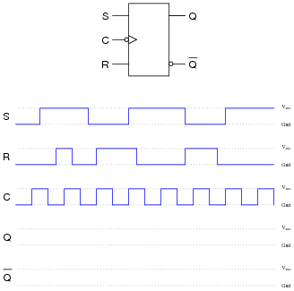
|
|
|
|
Notes:
In order to successfully answer this question, students will have to identify what the "bubble" means on the clock input, and relate that to the timing diagram. Ask your students to share any tips they may have regarding the analysis of timing diagrams, specifically what points in the diagram are critical (i.e. what points in time are the only points where the outputs may actually change states).
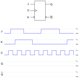
Question 12:
An extremely popular variation on the theme of an S-R flip-flop is the so-called J-K flip-flop circuit shown here:
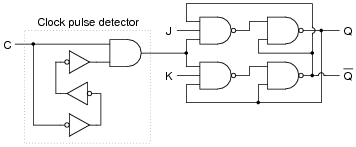
|
|
Note that an S-R flip-flop becomes a J-K flip-flop by adding another layer of feedback from the outputs back to the enabling NAND gates (which are now three-input, instead of two-input). What does this added feedback accomplish? Express your answer in the form of a truth table.
One way to consider the feedback lines going back to the first NAND gates is to regard them as extra enable lines, with the Q and [`Q] outputs selectively enabling just one of those NAND gates at a time.
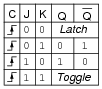
|
|
Follow-up question: comment on the difference between this truth table, and the truth table for an S-R flip-flop. Are there any operational advantages you see to J-K flip-flops over S-R flip-flops that makes them so much more popular?
Notes:
I have found that J-K flip-flop circuits are best analyzed by setting up input conditions (1's and 0's) on a schematic diagram, and then following all the gate output changes at the next clock pulse transition. A technique that really works well in the classroom for doing this is to project a schematic diagram on a clean whiteboard using an overhead projector or computer projector, then writing the 1 and 0 states with pen on the board. This allows you to quickly erase the 1's and 0's after each analysis without having to re-draw the schematic diagram. As always, I recommend you have students actually do the writing, with you taking the role of a coach, helping them rather than simply doing the thinking for them.
Question 13:
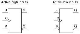
Determine what input conditions are necessary to set, reset, and toggle these two J-K flip-flops:
|
|
For the J-K flip-flop with active-high inputs:
- �
- Set by . . .
- �
- Reset by . . .
- �
- Toggle by . . .
For the J-K flip-flop with active-low inputs:
- �
- Set by . . .
- �
- Reset by . . .
- �
- Toggle by . . .
- �
- Set by activating J, deactivating K, and clocking C.
- �
- Reset by activating K, deactivating J, and clocking C.
- �
- Toggle by activating J and K simultaneously, and clocking C.
Specifically, though, here is what you would need to do to each flip-flop, stated in terms of "high" and "low" logic states:
For the J-K flip-flop with active-high inputs:
- �
- Set by making J high, K low, and C transition from low to high.
- �
- Reset by making K high, J low, and C transition from low to high.
- �
- Toggle by making J high, K high, and C transition from low to high.
For the J-K flip-flop with active-low inputs:
- �
- Set by making K high, J low, and C transition from high to low.
- �
- Reset by making J high, K low, and C transition from high to low.
- �
- Toggle by making J low, K low, and C transition from high to low.
Notes:
This question reviews the basic modes of J-K flip-flops, as well as the significance of active-low inputs.
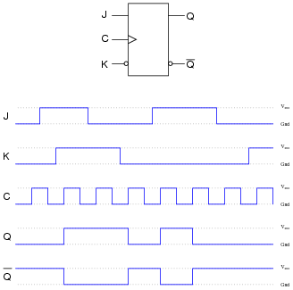
Question 14:
Determine the output states for this J-K flip-flop, given the pulse inputs shown:
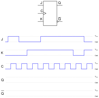
|
|
|
|
Notes:
Ask students to identify those regions on the timing diagram where the flip-flop is being set, reset, and toggled.
Question 15:
Determine the output states for this D flip-flop, given the pulse inputs shown:
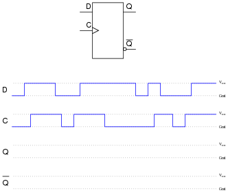
|
|
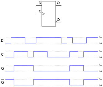
|
|
Notes:
Ask students to identify those regions on the timing diagram where the flip-flop is being set and reset.
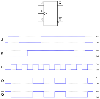
Question 16:
Determine the output states for this J-K flip-flop, given the pulse inputs shown:
|
|
|
|
Notes:
Ask students to identify those regions on the timing diagram where the flip-flop is being set, reset, and toggled.
Question 17:
Flip-flops often come equipped with asynchronous input lines as well as synchronous input lines. This J-K flip-flop, for example, has both "preset" and "clear" asynchronous inputs:
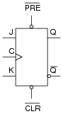
|
|
Describe the functions of these inputs. Why would we ever want to use them in a circuit? Explain what the ßynchronous" inputs are, and why they are designated by that term.
Also, note that both of the asynchronous inputs are active-low. As a rule, asynchronous inputs are almost always active-low rather than active-high, even if all the other inputs on the flip-flop are active-high. Why do you suppose this is?
As for why the asynchronous inputs are active-low, I won't directly give you the answer. But I will give you a hint: consider a TTL implementation of this flip-flop.
Notes:
Note to your students that sometimes the Preset and Clear inputs are called direct set and direct reset, respectively. Review with your students what it means for an input to be äctive-low" versus äctive-high." Ask them what consequences might arise if a circuit designer misunderstood the input states and failed to provide the right type of signal to the circuit.
Question 18:
A scientist is using a microprocessor system to monitor the boolean ("high" or "low") status of a particle sensor in her high-speed nuclear experiment. The problem is, the nuclear events detected by the sensor come and go much faster than the microprocessor is able to sample them. Simply put, the pulses output by the sensor are too brief to be "caught" by the microprocessor every time:
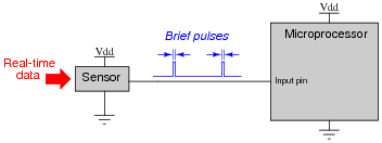
|
|
She asks several technicians to try and fix the problem. One tries altering the microprocessor's program to achieve a faster sampling rater, to no avail. Another recalibrates the particle sensor to react slower, but this only results in missed data (because the real world data does not slow down accordingly!). No solution tried so far works, because the fundamental problem is that the microprocessor is just too slow to "catch" the extremely short pulse events coming from the particle sensor. What is required is some kind of external circuit to "read" the sensor's state at the leading edge of a sample pulse, and then hold that digital state long enough for the microprocessor to reliably register it.
Finally, another electronics technician comes along and proposes this solution, but then goes on vacation, leaving you to implement it:
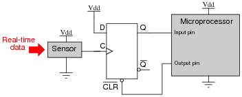
|
|
Explain how this D-type flip-flop works to solve the problem, and what action the microprocessor has to take on the output pin to make the flip-flop function as a detector for multiple pulses.
Challenge question: what logic family of flip-flop would you recommend be used for this application, given the need for extremely fast response? Don't just say "TTL," either. Research the fastest modern logic family in current manufacture!
Notes:
This is a very practical application for a D-type flip-flop, and also an introduction to one of the pitfalls of microprocessor-based data acquisition systems. Explain to your students that the finite time required for a microprocessor to cycle through its program may lead to conditions such as this where real-time events are missed because the microprocessor was "busy" doing other things at the time.
Question 19:
Identify at least one component fault that would cause the flip-flop to indicate "clockwise" all the time, regardless of encoder motion:
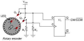
|
|
For each of your proposed faults, explain why it will cause the described problem.
- �
- Phototransistor Q1 failed shorted.
- �
- Resistor R2 failed open.
- �
- Flipflop U1 output failed high.
Follow-up question: explain why the presence of ambient light near the phototransistors could also cause this problem to occur.
Notes:
Be sure to discuss with your students the reasons why their proposed faults would cause the stated problem.
Question 20:
Suppose a student wants to build a sound-controlled lamp control circuit, whereby a single clap or other loud burst of noise turns the lamp on, and another single clap turns it off. The sound-detection and lamp-drive circuitry is shown here:
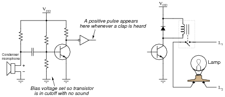
|
|
Add a J-K flip-flop to this schematic diagram to implement the toggling function.
|
|
Notes:
Some students may ask whether there is any significance to using the [`Q] output rather than the Q. Discuss this with your students: whether they think it will make any difference, or if it was just an arbitrary choice made by the circuit's designer. Then, ask them how they would go about proving their judgment.
There are plenty of "what if" failure scenarios you could ask your students about here, challenging them to analyze this circuit with a troubleshooting perspective. If time permits, have some fun with this.
Question 21:
If the clock frequency driving this flip-flop is 240 Hz, what is the frequency of the flip-flop's output signals (either Q or [`Q])?
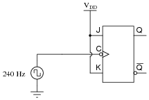
|
|
Follow-up question: how could you use another flip-flop to obtain a square-wave signal of 60 Hz from this circuit?
Notes:
Ask your students to think of some practical applications for this type of circuit. For those who are musically inclined, ask them what the musical relationship is between notes whose frequencies are an exact 2:1 ratio (hint: it's the same interval as eight white keys on a piano keyboard). How could a circuit such as this possibly be used in a musical synthesizer?
Question 22:
The flip-flop circuit shown here is classified as synchronous because both flip-flops receive clock pulses at the exact same time:
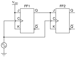
|
|
Define the following parameters:
- �
- Set-up time
- �
- Hold time
- �
- Propagation delay time
- �
- Minimum clock pulse duration
Then, explain how each of these parameters is relevant in the circuit shown.
Notes:
I could have simply asked students to define the terms, but where's the fun in that? Seriously, though, these concepts will make far more sense to students when they are viewed in a practical context. After all, the whole purpose of teaching these concepts is so students will be able to apply them, right?
Question 23:
Locate a manufacturer's datasheet for a flip-flop IC, and research the following parameters:
- �
- Flip-flop type (S-R, D, J-K)
- �
- Part number
- �
- ANSI/IEEE standard symbol
- �
- How many asynchronous inputs
- �
- Minimum setup and hold times (shown in timing diagrams)
Notes:
In case students claim they "could not find any parts to research," suggest the following:
- �
- 74107
- �
- 74109
- �
- 74112
- �
- 40174
- �
- 40175
Question 24:
Although the toggle function of the J-K flip-flop is one of its most popular uses, this is not the only type of flip-flop capable of performing a toggle function. Behold the surprisingly versatile D-type flip-flop configured to do the same thing:
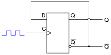
|
|
Explain how this circuit performs the "toggle" function more commonly associated with J-K flip-flops.
Notes:
The main purpose of this question is to get students to see that toggling is not the exclusive domain of J-K flip-flops. This fact may be particularly handy to know if one needs a toggle function in a circuit but only has a D-type flip-flop available, not a J-K flip-flop.
Question 25:
A student has an idea to make a J-K flip-flop toggle: why not just connect the J, K, and Clock inputs together and drive them all with the same square-wave pulse? If the inputs are active-high and the clock is positive edge-triggered, the J and K inputs should both go "high" at the same moment the clock signal transitions from low to high, thus establishing the necessary conditions for a toggle (J=1, K=1, clock transition):
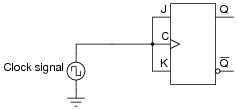
|
|
Unfortunately, the J-K flip-flop refuses to toggle when this circuit is built. No matter how many clock pulses it receives, the Q and [`Q] outputs remain in their original states - the flip-flop remains "latched." Explain the practical reason why the student's flip-flop circuit idea will not work.
Notes:
The purpose of this question is to get students to think about setup time, and to see its importance by providing a scenario where the circuit will not work because this parameter has been ignored.
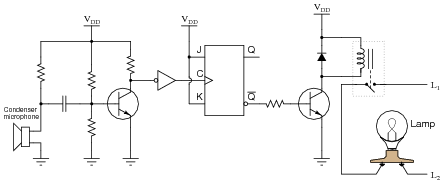
Question 26:
Predict how the operation of this sound-activated lamp circuit will be affected as a result of the following faults. Consider each fault independently (i.e. one at a time, no multiple faults):
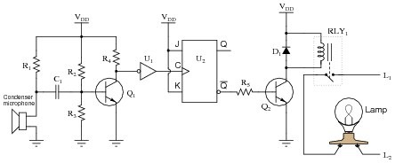
|
|
- �
- Resistor R1 fails open:
- �
- Resistor R3 fails open:
- �
- Diode D1 fails open:
- �
- Transistor Q2 fails shorted between collector and emitter:
- �
- Solder bridge past resistor R5:
For each of these conditions, explain why the resulting effects will occur.
- �
- Resistor R1 fails open: Lamp status does not change.
- �
- Resistor R3 fails open: Lamp status does not change.
- �
- Diode D1 fails open: Circuit works fine for a few cycles, then fails with the lamp either remaining on or remaining off (due to failed transistor Q2).
- �
- Transistor Q2 fails shorted between collector and emitter: Lamp remains on.
- �
- Solder bridge past resistor R5: Possible failure of flip-flop U2 or transistor Q2 after extended periods of time with the lamp on.
Notes:
The purpose of this question is to approach the domain of circuit troubleshooting from a perspective of knowing what the fault is, rather than only knowing what the symptoms are. Although this is not necessarily a realistic perspective, it helps students build the foundational knowledge necessary to diagnose a faulted circuit from empirical data. Questions such as this should be followed (eventually) by other questions asking students to identify likely faults based on measurements.