Insulated gate field-effect transistors
Question 1:
| Don't just sit there! Build something!! |
Learning to mathematically analyze circuits requires much study and practice. Typically, students practice by working through lots of sample problems and checking their answers against those provided by the textbook or the instructor. While this is good, there is a much better way.
You will learn much more by actually building and analyzing real circuits, letting your test equipment provide the änswers" instead of a book or another person. For successful circuit-building exercises, follow these steps:
- 1.
- Carefully measure and record all component values prior to circuit construction, choosing resistor values high enough to make damage to any active components unlikely.
- 2.
- Draw the schematic diagram for the circuit to be analyzed.
- 3.
- Carefully build this circuit on a breadboard or other convenient medium.
- 4.
- Check the accuracy of the circuit's construction, following each wire to each connection point, and verifying these elements one-by-one on the diagram.
- 5.
- Mathematically analyze the circuit, solving for all voltage and current values.
- 6.
- Carefully measure all voltages and currents, to verify the accuracy of your analysis.
- 7.
- If there are any substantial errors (greater than a few percent), carefully check your circuit's construction against the diagram, then carefully re-calculate the values and re-measure.
When students are first learning about semiconductor devices, and are most likely to damage them by making improper connections in their circuits, I recommend they experiment with large, high-wattage components (1N4001 rectifying diodes, TO-220 or TO-3 case power transistors, etc.), and using dry-cell battery power sources rather than a benchtop power supply. This decreases the likelihood of component damage.
As usual, avoid very high and very low resistor values, to avoid measurement errors caused by meter "loading" (on the high end) and to avoid transistor burnout (on the low end). I recommend resistors between 1 kW and 100 kW.
One way you can save time and reduce the possibility of error is to begin with a very simple circuit and incrementally add components to increase its complexity after each analysis, rather than building a whole new circuit for each practice problem. Another time-saving technique is to re-use the same components in a variety of different circuit configurations. This way, you won't have to measure any component's value more than once.
Notes:
It has been my experience that students require much practice with circuit analysis to become proficient. To this end, instructors usually provide their students with lots of practice problems to work through, and provide answers for students to check their work against. While this approach makes students proficient in circuit theory, it fails to fully educate them.
Students don't just need mathematical practice. They also need real, hands-on practice building circuits and using test equipment. So, I suggest the following alternative approach: students should build their own "practice problems" with real components, and try to mathematically predict the various voltage and current values. This way, the mathematical theory "comes alive," and students gain practical proficiency they wouldn't gain merely by solving equations.
Another reason for following this method of practice is to teach students scientific method: the process of testing a hypothesis (in this case, mathematical predictions) by performing a real experiment. Students will also develop real troubleshooting skills as they occasionally make circuit construction errors.
Spend a few moments of time with your class to review some of the "rules" for building circuits before they begin. Discuss these issues with your students in the same Socratic manner you would normally discuss the worksheet questions, rather than simply telling them what they should and should not do. I never cease to be amazed at how poorly students grasp instructions when presented in a typical lecture (instructor monologue) format!
A note to those instructors who may complain about the "wasted" time required to have students build real circuits instead of just mathematically analyzing theoretical circuits:
What is the purpose of students taking your course?
If your students will be working with real circuits, then they should learn on real circuits whenever possible. If your goal is to educate theoretical physicists, then stick with abstract analysis, by all means! But most of us plan for our students to do something in the real world with the education we give them. The "wasted" time spent building real circuits will pay huge dividends when it comes time for them to apply their knowledge to practical problems.
Furthermore, having students build their own practice problems teaches them how to perform primary research, thus empowering them to continue their electrical/electronics education autonomously.
In most sciences, realistic experiments are much more difficult and expensive to set up than electrical circuits. Nuclear physics, biology, geology, and chemistry professors would just love to be able to have their students apply advanced mathematics to real experiments posing no safety hazard and costing less than a textbook. They can't, but you can. Exploit the convenience inherent to your science, and get those students of yours practicing their math on lots of real circuits!
Question 2:
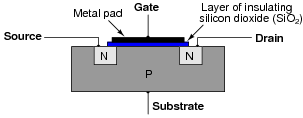
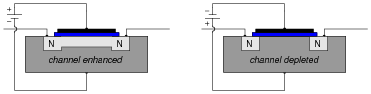
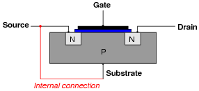
The following illustration is a cross-section of an insulated gate field-effect transistor, sometimes referred to as an IGFET:
|
|
Explain what happens when a positive voltage is applied to the gate (with reference to the substrate), with regard to electrical conductivity between the source and drain:

|
|
|
|
Notes:
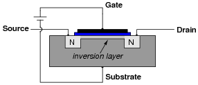
Ask your students to explain how the inversion layer forms, and what it means for source-drain conduction if no inversion layer is present.
Discuss with your students the fact that this inversion layer is incredibly thin; so this that it is often referred to as a two-dimensional ßheet" of charge carriers.
Also mention to your students that although ÏGFET" is the general term for such a device, "MOSFET" is more commonly used as a designator due to the device's history.
Question 3:
The letters "MOS" in the acronym "MOSFET" stand for "Metal Oxide Semiconductor". Describe what this means, in reference to the construction of a MOSFET.
Follow-up question: MOSFETs are sometimes referred to as ÏGFETs". Explain what this other acronym stands for, and how it means the same thing as "MOSFET".
Notes:
Explain to your students that IGFET is a more general term than MOSFET, as silicon dioxide is not the only suitable material from which to make an insulating layer for the gate.
Question 4:
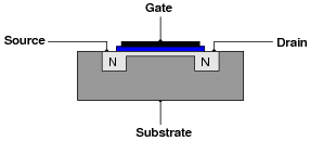
Some types of MOSFETs have a source-drain channel already formed with no applied gate voltage:
|
|
Explain what happens to source-drain conductivity with each of the following applied gate-to-substrate voltages. Modify the illustrations if necessary:
|
|
|
|
Notes:
Ask your students to contrast the behavior of this type of MOSFET against the behavior of the type that requires a gate voltage to create an inversion layer.
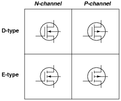
Question 5:
There are two general classes of MOSFETs: MOSFETs that conduct with no applied gate voltage, and MOSFETs that require a gate voltage to be applied for conduction. What are each of these MOSFET types called, and what are their respective schematic symbols?
Each of the symbols for these different types of MOSFETs hold clues to the transistor types they represent. Explain how the symbols hint at the characteristics of their respective transistor types.
|
|
Notes:
The part of this question asking about clues within the transistor symbols is very important. It will be far easier for your students to remember the function of each transistor type if they are able to recognize clues in the symbolism.
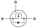
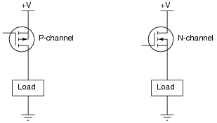
Question 6:
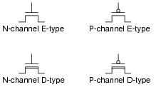
Identify these schematic symbols:
|
|
|
|
Notes:
The "bubble" symbol on the gate of the P-channel devices is reminiscent of inversion bubbles used on logic gate symbols. I'm assuming that your students will not have studied logic gates at this point, so this is a foreshadowing of things to come!
Question 7:
Field effect transistors are classified as majority carrier devices. Explain why.
Review question: in contrast, why are bipolar junction transistors considered minority carrier devices?
Notes:
Ask your students what type of transistor operates on a minority carrier principle, as opposed to field-effect transistors.
Question 8:
Bipolar junction transistors (BJTs) are considered "normally-off" devices, because their natural state with no signal applied to the base is no conduction between emitter and collector, like an open switch. Are insulate-gate field-effect transistors (IGFETs) considered the same? Why or why not?
Notes:
Ask your students to elaborate on the answer given. Do not accept a mindless recitation of the answer, that ït depends on how they're manufactured," but rather demand that some sort of explanation be given as to why an IGFET would be normally-on versus normally-off.
Question 9:
The typical amount of current through a MOSFET gate terminal is far less than the typical amount of current through a BJT base terminal, for similar controlled currents (drain or collector, respectively). Explain what it is about the construction and/or use of the MOSFET that limits the input current to almost nothing during normal operation.
Notes:
If need be, refer back to a "cut-away" diagram of a MOSFET to help your students understand why the input impedance of a MOSFET is what it is.
Question 10:
Metal Oxide Field-Effect Transistors (MOSFETs) differ in behavior from Bipolar Junction Transistors (BJTs) in several ways. Address each one of these behavioral aspects in your answer:
- �
- Current gain
- �
- Conduction with no input (gate/base) signal
- �
- Polarization
BJTs are normally-off devices, whereas a MOSFET may either be normally-on or normally-off depending on its manufacture.
MOSFETs can pass current from source to drain, or from drain to source with equal ease. BJTs can only pass current from emitter to collector in one direction.
Notes:
For each one of these behavioral aspects, discuss with your students exactly why the two transistors types differ.
Question 11:
E-type MOSFETs are normally-off devices just like bipolar junction transistors, the natural state of their channels strongly resisting the passage of electric currents. Thus, a state of conduction will only occur on command from an external source.
Explain what must be done to an E-type MOSFET, specifically, to drive it into a state of conduction (where a channel forms to conduct current between source and drain).
Notes:
This is perhaps the most important question your students could learn to answer when first studying E-type MOSFETs. What, exactly, is necessary to turn one on? Have your students draw diagrams to illustrate their answers as they present in front of the class.
Ask them specifically to identify what polarity of VGS would have to be applied to turn on an N-channel E-type MOSFET, and also a P-channel E-type MOSFET.
Question 12:
D-type MOSFETs are normally-on devices just like junction field-effect transistors, the natural state of their channels being passable to electric currents. Thus, a state of cutoff will only occur on command from an external source.
Explain what must be done to an D-type MOSFET, specifically, to drive it into a state of cutoff (where the channel is fully depleted).
Follow-up question: unlike JFETs, D-type MOSFETs may be safely ënhanced" beyond the conductivity of their natural state. Describe what is necessary to "command" a D-type MOSFET to conduct better than it naturally does.
Notes:
This is perhaps the most important question your students could learn to answer when first studying D-type MOSFETs. What, exactly, is necessary to turn one off? Have your students draw diagrams to illustrate their answers as they present in front of the class.
Ask them specifically to identify what polarity of VGS would have to be applied to turn off an N-channel D-type MOSFET, and also a P-channel D-type MOSFET.
Question 13:
Metal Oxide Field-Effect Transistors (MOSFETs) differ in some regards from Junction Field-Effect Transistors (JFETs). Explain in your own words what the difference(s) is/are.
Notes:
Despite their many similarities, MOSFETs and JFETs are not identical. Ask your students to explain why the two types of transistor behave differently, not just recite differences read from a textbook or other reference.
Question 14:
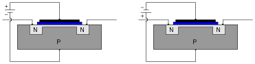
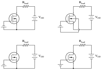
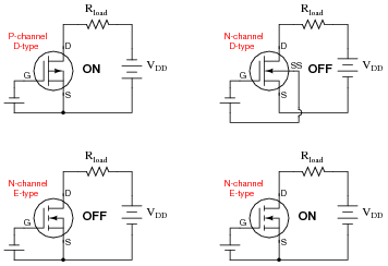
Identify each type of MOSFET (whether it is N-channel or P-channel, D-type or E-type), label the terminals, and determine whether the MOSFET in each of these circuits will be turned on or off:
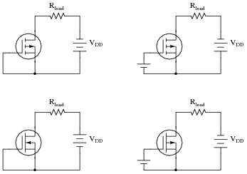
|
|
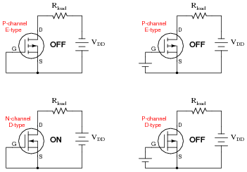
|
|
Follow-up question: which of these transistors is depleted and which is enhanced?
Notes:
It is very important for your students to understand what factor(s) in a circuit force a MOSFET to turn on or off. Some of the information contained in the diagrams is relevant to the determination of each transistor's status, and some is not.
Be sure to ask your students to explain their reasoning for each transistor's status. What factor, or combination of factors, is necessary to turn a MOSFET on, versus off?
Question 15:
Identify each type of MOSFET (whether it is N-channel or P-channel, D-type or E-type), label the terminals, and determine whether the MOSFET in each of these circuits will be turned on or off:
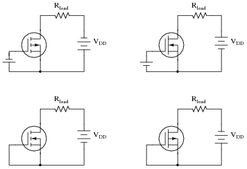
|
|
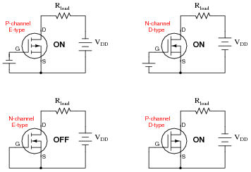
|
|
Follow-up question: which of these transistors is depleted and which is enhanced?
Notes:
It is very important for your students to understand what factor(s) in a circuit force a MOSFET to turn on or off. Some of the information contained in the diagrams is relevant to the determination of each transistor's status, and some is not.
Be sure to ask your students to explain their reasoning for each transistor's status. What factor, or combination of factors, is necessary to turn a MOSFET on, versus off?
Question 16:
Identify each type of MOSFET (whether it is N-channel or P-channel, D-type or E-type), label the terminals, and determine whether the MOSFET in each of these circuits will be turned on or off:
|
|
|
|
Follow-up question: which of these transistors is depleted and which is enhanced?
Notes:
It is very important for your students to understand what factor(s) in a circuit force a MOSFET to turn on or off. Some of the information contained in the diagrams is relevant to the determination of each transistor's status, and some is not.
Be sure to ask your students to explain their reasoning for each transistor's status. What factor, or combination of factors, is necessary to turn a MOSFET on, versus off?
Question 17:
Explain why a circuit designer would choose a MOSFET over a bipolar transistor for a certain application. What advantage(s) does a MOSFET have over a bipolar transistor?
Challenge question: prove your point by comparing parametric ratings from two transistor datasheets, one bipolar and the other an insulated-gate field effect. Be sure these two transistors have similar controlled current ratings (maximum collector current and drain current, respectively).
Notes:
Ask your students to explain what "drive current" means in terms of transistor ratings. Also, ask them to explain why MOSFETs do not require as much drive current as bipolar transistors. Challenge them to prove their point by a comparison of datasheets.
Is low drive current the only advantage that MOSFETs enjoy over bipolar transistors? Pose this question to your students, to see if they investigated these respective devices any further than the question demanded.
Question 18:
What does the term transconductance mean, with reference to a field-effect transistor? Is the transconductance function for an FET a linear or a nonlinear relationship? Explain why, making reference to an equation if at all possible to explain your answer.
Challenge question: what unit of measurement would be appropriate for expressing transconductance in?
Notes:
Transconductance is not just a parameter for JFETs, but also MOSFETs (IGFETs) and vacuum tubes. Any voltage-controlled current-regulating device has a transconductance value (though it may change over the operating range of the device, just as b changes over the operating range of a BJT).
Question 19:
The ßubstrate" connection in a MOSFET is often internally connected to the source, like this:
|
|
This turns the MOSFET from a four-terminal device into a three-terminal device, making it easier to use. One consequence of this internal connection, though, is the creation of a parasitic diode between the source and drain terminals: a PN junction that exists whether we want it to or not.
Add this parasitic diode to the MOSFET symbol shown here (representing the MOSFET cross-section shown above), and explain how its presence affects the transistor's use in a real circuit:

|
|
|
|
Follow-up question: how does the presence of this parasitic diode allow us to positively distinguish the source terminal from the gate terminal when identifying the terminals of a MOSFET with a multimeter?
Notes:
The presence of this diode is a very important concept for students to grasp, as it makes the MOSFET a unilateral device for most practical purposes. Discuss the significance of this diode, and contrast the characteristics of a three-terminal MOSFET against the characteristics of a three-terminal JFET, which is a truly bilateral device.
Question 20:
A technician is using a digital multimeter (with a "diode check" feature) to identify the terminals of a power MOSFET:
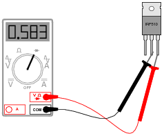
|
|
The technician obtains the following "diode check" voltage measurements, in this order:
- 1.
- Black lead on middle terminal, Red lead on right terminal = 0.583 volts (shown in illustration)
- 2.
- Red lead on middle terminal, Black lead on right terminal = O.L. (open)
- 3.
- Black lead on middle terminal, Red lead on left terminal = O.L. (open)
- 4.
- Black lead on middle terminal, Red lead on right terminal = 0.001 volts
- 5.
- Red lead on middle terminal, Black lead on right terminal = 0.001 volts
Explain why the fourth and fifth measurements are so different from the first and second, respectively, when they were taken between the same terminals on the MOSFET. Hint: this particular MOSFET is an N-channel, enhancement-type.
Follow-up question: where would the meter have to be connected in order to force the MOSFET into is off (cutoff) state?
Notes:
Field-effect transistors, by their very nature being voltage-activated devices with extremely high input impedance, are more difficult to identify than bipolar junction transistors because the meter's output in the "diode check" mode is sufficient to activate and de-activate them. This question showcases a practical example of this (the values actually came from real-life testing of an IRF510 transistor!).
Question 21:
An important consideration when working around circuits containing MOSFETs is electrostatic discharge, or ESD. Describe what this phenomenon is, and why it is an important consideration for MOSFET circuits.
Notes:
Be sure to ask students to explain the mechanism of transistor damage resulting from ESD, and to discuss the sheer magnitude of static voltages typically generated in dry-air conditions. If you have any microphotographs of IC damage from ESD, present a few of them during discussion time for your students' viewing pleasure.
Question 22:
Anti-static wrist straps are commonly worn by technicians when performing work on circuits containing MOSFETs. Explain how these straps are used, and how you would test one to ensure it is functioning properly.
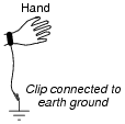
|
|
A simple ohmmeter test should reveal mega-ohm levels of resistance between the strap's skin contact point and the metal grounding clip.
Follow-up question: why is there resistance intentionally placed between the wrist strap and the grounding clip? What would be wrong with simply having a 0 W connection between the strap and earth ground (i.e. an uninterrupted length of wire)?
Notes:
A good question to ask your students is why anti-static protection is important when working with MOSFET devices. You should never assume this is obvious, unless the subject was covered in a question immediately previous to this one!
Your students should have an anti-static wrist strap as part of their regular tool collection. When discussing this question, it would be good to have students use their ohmmeters to verify the operation of their wrist straps.
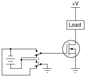
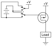
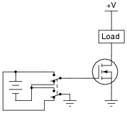
Question 23:
Complete the circuit, showing how the pushbutton switch could be connected to the gate of the MOSFET in order to exert control over the load:
|
|
|
|
Follow-up question: would you say this transistor sources current to the load, or sinks current from the load? Explain your answer.
Notes:
Discuss with your students why the circuit shown in the answer would not necessarily be practical, and work together to develop a better design.
Question 24:
Determine whether the load is energized or de-energized with the switch in the position shown. Also, identify whether the transistor is a depletion type or an enhancement type:

|
|
Notes:
Ask your students to explain how they figured out the state of the transistor in this circuit, and also what function the double-pole, double-throw (DPDT) switch performs. Incidentally, this DPDT switch wiring configuration is quite common in electrical and electronic circuits!
Question 25:
Determine whether the load is energized or de-energized with the switch in the position shown. Also, identify whether the transistor is a depletion type or an enhancement type:

|
|
Notes:
Ask your students to explain how they figured out the state of the transistor in this circuit, and also what function the double-pole, double-throw (DPDT) switch performs. Incidentally, this DPDT switch wiring configuration is quite common in electrical and electronic circuits!
Question 26:
Determine whether the load is energized or de-energized with the switch in the position shown. Also, identify whether the transistor is a depletion type or an enhancement type:
|
|
Notes:
Ask your students to explain how they figured out the state of the transistor in this circuit, and also what function the double-pole, double-throw (DPDT) switch performs. Incidentally, this DPDT switch wiring configuration is quite common in electrical and electronic circuits!
Question 27:
Determine whether the load is energized or de-energized with the switch in the position shown. Also, identify whether the transistor is a depletion type or an enhancement type:
|
|
Notes:
Ask your students to explain how they figured out the state of the transistor in this circuit, and also what function the double-pole, double-throw (DPDT) switch performs. Incidentally, this DPDT switch wiring configuration is quite common in electrical and electronic circuits!
Question 28:
Determine whether the load is energized or de-energized with the switch in the position shown. Also, identify whether the transistor is a depletion type or an enhancement type:
|
|
Notes:
Ask your students to explain how they figured out the state of the transistor in this circuit, and also what function the double-pole, double-throw (DPDT) switch performs. Incidentally, this DPDT switch wiring configuration is quite common in electrical and electronic circuits!
Question 29:
It is often necessary to have a power transistor source current to a load (provide a path from the positive supply voltage rail to the load) rather than sink current from the load (provide a path from the load to the negative voltage rail or ground), because one side of the load is already connected to ground:
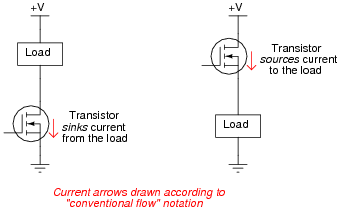
|
|
When the transistor sources current, it is often referred to as a high-side switch. Determine the driving voltage requirements for each of these high-side MOSFET switches; that is, determine what must be connected to the gate of each transistor to fully turn it on so that the load receives full power:
|
|
Follow-up question: discuss why the terms ßourcing" and ßinking" make the most sense when viewed from the perspective of conventional flow current notation. For contrast, here is the same circuit with the arrows drawn in the direction of electron flow:
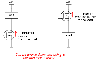
|
|
Challenge question: despite the more demanding gate drive requirements of the high-side N-channel MOSFET, these are often preferred over P-channel devices in practical circuit designs. Explain why. Hint: it has something to do with carrier mobility.
Notes:
This is a good exercise in determining proper gate voltage polarity (and magnitude), as well as introducing the concepts of current sourcing and sinking, and high-side switching. Be sure to spend time discussing the matter of sourcing versus sinking, as this will be of greater importance later in your students' studies (especially in logic gate circuit design).
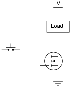
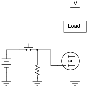
Question 30:
Draw the proper wire connections necessary for ënhancing" this MOSFET with the solar cell's voltage, so that the battery energizes the relay whenever there is sufficient light exposure on the solar cell:
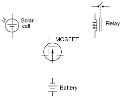
|
|
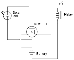
|
|
Challenge question: connect a commutating ("free-wheeling") diode into the circuit shown, so that inductive "kickback" from the relay de-energizing does not harm the MOSFET.
Notes:
Students should note that the circuit shown is not the only possible way a MOSFET could be used to turn a relay on. Often, the substrate (SS) and source (S) terminals of the MOSFET are made common with each other, so that the controlling and controlled circuits share a common point (usually the system "ground" point).
Ask your students what would happen if the battery's polarity were reversed.
Question 31:
Explain what will happen in this circuit when each pushbutton switch is individually actuated:
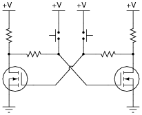
|
|
Can you think of any practical applications for a circuit like this?
If you experience difficulty analyzing this circuit's operation, imagine that one of the transistors is in the ön" state and the other is in the öff" state immediately after power-up. Then ask yourself what will happen when each pushbutton is actuated.
Notes:
Bistable latch, or multivibrator, circuits are quite useful and quite simple to implement with MOSFETs as this example demonstrates. Discuss some practical applications with your students, especially if they have not discovered a few applications of their own.
Question 32:
This circuit uses a combination of capacitance and resistance to produce a time delay when the pushbutton switch is released, causing the lamp to remain on for a short while after the switch opens:
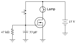
|
|
Calculate how long the lamp will remain on after the switch opens, assuming the MOSFET has a gate threshold (turn-on) voltage of VGS(th) = 4 volts.
Notes:
In order to solve this problem, students must apply their knowledge of capacitive discharge circuits to find the correct equation for time. Ask them how they set up the solution, and how they knew what equation(s) to use.
Question 33:
Predict how this circuit will be affected as a result of the following faults. Consider each fault independently (i.e. one at a time, no multiple faults):
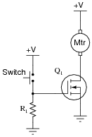
|
|
- �
- Transistor Q1 fails open (drain-to-source):
- �
- Transistor Q1 fails shorted (drain-to-source):
- �
- Resistor R1 fails open:
For each of these conditions, explain why the resulting effects will occur.
- �
- Transistor Q1 fails open (drain-to-source): Motor refuses to run.
- �
- Transistor Q1 fails shorted (drain-to-source): Motor runs all the time and will not turn off.
- �
- Resistor R1 fails open: Motor runs when switch is pressed, takes a long time to turn off when switch is released.
Notes:
The purpose of this question is to approach the domain of circuit troubleshooting from a perspective of knowing what the fault is, rather than only knowing what the symptoms are. Although this is not necessarily a realistic perspective, it helps students build the foundational knowledge necessary to diagnose a faulted circuit from empirical data. Questions such as this should be followed (eventually) by other questions asking students to identify likely faults based on measurements.
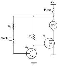
Question 34:
Predict how this circuit will be affected as a result of the following faults. Consider each fault independently (i.e. one at a time, no multiple faults):
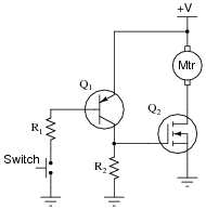
|
|
- �
- Transistor Q1 fails shorted (collector-to-emitter):
- �
- Transistor Q2 fails open (drain-to-source):
- �
- Resistor R1 fails open:
- �
- Resistor R2 fails open:
For each of these conditions, explain why the resulting effects will occur.
- �
- Transistor Q1 fails shorted (drain-to-source): Motor runs all the time and will not turn off.
- �
- Transistor Q2 fails open (drain-to-source): Motor refuses to run.
- �
- Resistor R1 fails open: Motor refuses to run.
- �
- Resistor R2 fails open: Motor runs when switch is pressed, takes a long time to turn off when switch is released.
Notes:
The purpose of this question is to approach the domain of circuit troubleshooting from a perspective of knowing what the fault is, rather than only knowing what the symptoms are. Although this is not necessarily a realistic perspective, it helps students build the foundational knowledge necessary to diagnose a faulted circuit from empirical data. Questions such as this should be followed (eventually) by other questions asking students to identify likely faults based on measurements.
Question 35:
Predict how this circuit will be affected as a result of the following faults. Consider each fault independently (i.e. one at a time, no multiple faults):
|
|
- �
- Transistor Q1 fails shorted (drain-to-source):
- �
- Transistor Q2 fails shorted (drain-to-source):
- �
- Resistor R1 fails open:
- �
- Resistor R2 fails open:
- �
- Solder bridge (short) past resistor R1:
For each of these conditions, explain why the resulting effects will occur.
- �
- Transistor Q1 fails shorted (drain-to-source): Motor refuses to run.
- �
- Transistor Q2 fails shorted (drain-to-source): Motor runs all the time and will not turn off.
- �
- Resistor R1 fails open: Motor runs all the time and will not turn off.
- �
- Resistor R2 fails open: Motor refuses to run.
- �
- Solder bridge (short) past resistor R1: Motor runs when switch is initially unpressed (as it should), but transistor Q1 will fail when switch is pressed. This may cause the motor to stop running or to never stop, depending on how Q1 fails. The fuse may also blow as a result.
Notes:
The purpose of this question is to approach the domain of circuit troubleshooting from a perspective of knowing what the fault is, rather than only knowing what the symptoms are. Although this is not necessarily a realistic perspective, it helps students build the foundational knowledge necessary to diagnose a faulted circuit from empirical data. Questions such as this should be followed (eventually) by other questions asking students to identify likely faults based on measurements.
Question 36:
A very useful MOSFET circuit is the bilateral switch, an example shown here for you to analyze:
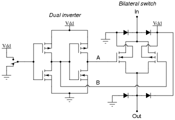
|
|
The "dual inverter" circuit simply ensures the two control lines A and B will always be opposite polarities (one at Vdd potential, the other at ground potential).
What is the purpose of a "bilateral switch" circuit? Hint: there are two integrated circuit implementations of the bilateral switch - the 4016 and the 4066. Investigate the datasheets for these integrated circuits to learn more!
Notes:
If your students have not yet learned about digital transistor circuits, this would be a good time to introduce the concept of "high" and "low" logic states, in this case as control signals to the bilateral switch cell.
Ask your students what the purpose of a bilateral switch might be, since we already have mechanical switches capable of switching almost any type of electrical signal known.
Question 37:
A special type of insulated-gate field-effect transistor is the dual gate MOSFET, shown here:

|
|
Draw a schematic diagram using normal (single-gate) MOSFETs, equivalent to this dual-gate MOSFET.
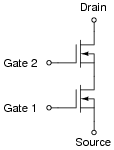
|
|
Notes:
A pretty simple answer to this question, but the real purpose is to challenge students to think of complex circuit elements in terms of equivalent circuits comprised of simple, idealized components.
Question 38:
|
A potential problem for power MOSFETs is [dv/dt] induced turn-on. Explain why a MOSFET may turn on when it's not supposed to, given an excessive [dv/dt] condition.
Challenge question: draw an equivalent schematic diagram showing the parasitic CGD capacitance, and write the equation relating capacitive current to instantaneous voltage change over time.
Notes:
This question is a good review of capacitor theory and calculus notation. Ask your students to explain exactly what [dv/dt] means, and how it relates to current in a circuit containing capacitance.
The problem of dv/dt induced turn-on is not unique to power MOSFETs. Various thyristors, most notably SCRs and TRIACs, also exhibit this problem.
Question 39:
Find one or two real insulated-gate field-effect transistors and bring them with you to class for discussion. Identify as much information as you can about your transistors prior to discussion:
- �
- Terminal identification (which terminal is gate, source, drain)
- �
- Continuous power rating
- �
- Typical transconductance
Note: be careful to keep your transistors in anti-static foam as much as possible, to avoid damage to the gate from electrostatic discharge.
Notes:
The purpose of this question is to get students to kinesthetically interact with the subject matter. It may seem silly to have students engage in a ßhow and tell" exercise, but I have found that activities such as this greatly help some students. For those learners who are kinesthetic in nature, it is a great help to actually touch real components while they're learning about their function. Of course, this question also provides an excellent opportunity for them to practice interpreting component markings, use a multimeter, access datasheets, etc.