Negative feedback opamp circuits
Question 1:
| Don't just sit there! Build something!! |
Learning to mathematically analyze circuits requires much study and practice. Typically, students practice by working through lots of sample problems and checking their answers against those provided by the textbook or the instructor. While this is good, there is a much better way.
You will learn much more by actually building and analyzing real circuits, letting your test equipment provide the änswers" instead of a book or another person. For successful circuit-building exercises, follow these steps:
- 1.
- Carefully measure and record all component values prior to circuit construction.
- 2.
- Draw the schematic diagram for the circuit to be analyzed.
- 3.
- Carefully build this circuit on a breadboard or other convenient medium.
- 4.
- Check the accuracy of the circuit's construction, following each wire to each connection point, and verifying these elements one-by-one on the diagram.
- 5.
- Mathematically analyze the circuit, solving for all voltage and current values.
- 6.
- Carefully measure all voltages and currents, to verify the accuracy of your analysis.
- 7.
- If there are any substantial errors (greater than a few percent), carefully check your circuit's construction against the diagram, then carefully re-calculate the values and re-measure.
Avoid using the model 741 op-amp, unless you want to challenge your circuit design skills. There are more versatile op-amp models commonly available for the beginner. I recommend the LM324 for DC and low-frequency AC circuits, and the TL082 for AC projects involving audio or higher frequencies.
As usual, avoid very high and very low resistor values, to avoid measurement errors caused by meter "loading". I recommend resistor values between 1 kW and 100 kW.
One way you can save time and reduce the possibility of error is to begin with a very simple circuit and incrementally add components to increase its complexity after each analysis, rather than building a whole new circuit for each practice problem. Another time-saving technique is to re-use the same components in a variety of different circuit configurations. This way, you won't have to measure any component's value more than once.
Notes:
It has been my experience that students require much practice with circuit analysis to become proficient. To this end, instructors usually provide their students with lots of practice problems to work through, and provide answers for students to check their work against. While this approach makes students proficient in circuit theory, it fails to fully educate them.
Students don't just need mathematical practice. They also need real, hands-on practice building circuits and using test equipment. So, I suggest the following alternative approach: students should build their own "practice problems" with real components, and try to mathematically predict the various voltage and current values. This way, the mathematical theory "comes alive," and students gain practical proficiency they wouldn't gain merely by solving equations.
Another reason for following this method of practice is to teach students scientific method: the process of testing a hypothesis (in this case, mathematical predictions) by performing a real experiment. Students will also develop real troubleshooting skills as they occasionally make circuit construction errors.
Spend a few moments of time with your class to review some of the "rules" for building circuits before they begin. Discuss these issues with your students in the same Socratic manner you would normally discuss the worksheet questions, rather than simply telling them what they should and should not do. I never cease to be amazed at how poorly students grasp instructions when presented in a typical lecture (instructor monologue) format!
A note to those instructors who may complain about the "wasted" time required to have students build real circuits instead of just mathematically analyzing theoretical circuits:
What is the purpose of students taking your course?
If your students will be working with real circuits, then they should learn on real circuits whenever possible. If your goal is to educate theoretical physicists, then stick with abstract analysis, by all means! But most of us plan for our students to do something in the real world with the education we give them. The "wasted" time spent building real circuits will pay huge dividends when it comes time for them to apply their knowledge to practical problems.
Furthermore, having students build their own practice problems teaches them how to perform primary research, thus empowering them to continue their electrical/electronics education autonomously.
In most sciences, realistic experiments are much more difficult and expensive to set up than electrical circuits. Nuclear physics, biology, geology, and chemistry professors would just love to be able to have their students apply advanced mathematics to real experiments posing no safety hazard and costing less than a textbook. They can't, but you can. Exploit the convenience inherent to your science, and get those students of yours practicing their math on lots of real circuits!
Question 2:
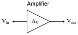
The voltage gain of a single-ended amplifier is defined as the ratio of output voltage to input voltage:
|
|
|
Often voltage gain is defined more specifically as the ratio of output voltage change to input voltage change. This is generally known as the AC voltage gain of an amplifier:
|
In either case, though, gain is a ratio of a single output voltage to a single input voltage.
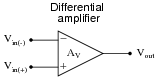
How then do we generally define the voltage gain of a differential amplifier, where there are two inputs, not just one?
|
|
Notes:
This is a very important concept for students to grasp, especially before they proceed to study operational amplifiers, which are nothing more than differential amplifiers with extremely high voltage gains.
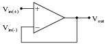
Question 3:
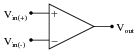
Write the transfer function (input/output equation) for an operational amplifier with an open-loop voltage gain of 100,000. In other words, write an equation describing the output voltage of this op-amp (Vout) for any combination of input voltages (Vin(+) and Vin(-)):
|
|
Notes:
The concept of a "transfer function" is very useful, and this may be your students' first exposure to the idea. It is a phrase used quite often in engineering applications, and may denote an equation, a table of numbers, or a graph.
In this particular question, it is important that students know how to derive and use the basic transfer function for a differential amplifier. Challenge your students to express this function in a more general form, so that calculations may be made with different open-loop voltage gains.
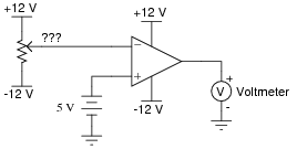
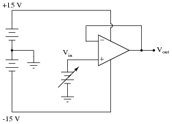
Question 4:
How much voltage would have to be "dialed up" at the potentiometer in order to stabilize the output at exactly 0 volts, assuming the opamp has no input offset voltage?
|
|
Notes:
This question is a basic review of an ideal differential amplifier's function. Ask your students what voltage must be "dialed up" at the potentiometer to produce 0 volts at the output of the op-amp for several different voltages at the other input. If they don't understand at first, they soon will after discussing these alternate scenarios.
Question 5:
An op-amp has +3 volts applied to the inverting input and +3.002 volts applied to the noninverting input. Its open-loop voltage gain is 220,000. Calculate the output voltage as predicted by the following formula:
|
How much differential voltage (input) is necessary to drive the output of the op-amp to a voltage of -4.5 volts?
Follow-up question: is this voltage figure realistic? Is it possible for an op-amp such as the model 741 to output 440 volts? Why or why not?
The differential input voltage necessary to drive the output of this op-amp to -4.5 volts is -20.455 mV.
Follow-up question: what does it mean for the input voltage differential to be negative 20.455 microvolts? Provide an example of two input voltages (Vin(+) and Vin(-)) that would generate this much differential voltage.
Notes:
Obviously, there are limitations to the op-amp formula for calculating output voltage, given input voltages and open-loop voltage gain. Students need to realize the practical limits of an op-amp's output voltage range, and what sets those limits.
Question 6:
A very important concept in electronics is that of negative feedback. This is an extremely important concept to grasp, as a great many electronic systems exploit this principle for their operation and cannot be properly understood without a comprehension of it.
However important negative feedback might be, it is not the easiest concept to understand. In fact, it is quite a conceptual leap for some. The following is a list of examples - some electronic, some not - exhibiting negative feedback:
- �
- A voltage regulating circuit
- �
- An auto-pilot system for an aircraft or boat
- �
- A thermostatic temperature control system ("thermostat")
- �
- Emitter resistor in a BJT amplifier circuit
- �
- Lenz's Law demonstration (magnetic damping of a moving object)
- �
- Body temperature of a mammal
- �
- Natural regulation of prices in a free market economy (Adam Smith's ïnvisible hand")
- �
- A scientist learning about the behavior of a natural system through experimentation.
For each case, answer the following questions:
- �
- What variable is being stabilized by negative feedback?
- �
- How is the feedback taking place (step by step)?
- �
- What would the system's response be like if negative feedback were not present?
- �
- What variable is being stabilized by negative feedback?
- Output voltage.
- �
- How is the feedback taking place (step by step)?
- When output voltage rises, the system takes action to drop more voltage internally, leaving less for the output.
- �
- What would the system's response be like if negative feedback were not present?
- Without negative feedback, the output voltage would rise and fall directly with the input voltage, and inversely with the load current.
Notes:
It is difficult to overstate the importance of grasping negative feedback in the study of electronics. So many different types of systems depend on it for their operation that it cannot be omitted from any serious electronics curriculum. Yet I see many textbooks fail to explore this principle in adequate depth, or discuss it in a mathematical sense only where students are likely to miss the basic concept because they will be too focused on solving the equations.
Question 7:
Write the transfer function (input/output equation) for an operational amplifier with an open-loop voltage gain of 100,000, and the inverting input connected directly to its output terminal. In other words, write an equation describing the output voltage of this op-amp (Vout) for any given input voltage at the noninverting input (Vin(+)):
|
|
Then, once you have an equation written, solve for the over-all voltage gain (AV = [(Vout)/(Vin(+))]) of this amplifier circuit, and calculate the output voltage for a noninverting input voltage of +6 volts.
|
(I've left it up to you to perform the algebraic simplification here!)
|
For an input voltage of +6 volts, the output voltage will be +5.99994 volts.
Notes:
The significant point of this question is that students see the over-all voltage gain of the opamp radically attenuated from 100,000 to approximately 1. What is not so evident is just how stable this new voltage gain is, which is one of the purposes for employing negative feedback.
Question 8:
How much effect will a change in the op-amp's open-loop voltage gain have on the overall voltage gain of a negative-feedback circuit such as this?
|
|
If the open-loop gain of this operational amplifier were to change from 100,000 to 200,000, for example, how big of an effect would it have on the voltage gain as measured from the noninverting input to the output?
Follow-up question: what advantage is there in building voltage amplifier circuits in this manner, applying negative feedback to a "core" amplifier with very high intrinsic gain?
Notes:
Work with your students to calculate a few example scenarios, with the old open-loop gain versus the new open-loop gain. Have the students validate their conclusions with numbers!
Negative feedback is an extremely useful engineering principle, and one that allows us to build very precise amplifiers using imprecise components. Credit for this idea goes to Harold Black, an electrical engineer, in 1920's. Mr. Black was looking for a way to improve the linearity and stability of amplifiers in telephone systems, and (as legend has it) the idea came to him in a flash of insight as he was commuting on a ferry boat.
An interesting historical side-note is that Black's 1928 patent application was initially rejected on the grounds that he was trying to submit a perpetual motion device! The concept of negative feedback in an amplifier circuit was so contrary to established engineering thought at the time, that Black experienced significant resistance to the idea within the engineering community. The United States patent office, on the other hand, was inundated with fraudulent "perpetual motion" claims, and so dismissed Black's invention at first sight.
Question 9:
Complete the table of voltages for this opamp "voltage follower" circuit:
|
|
-
Vin Vout
0 volts 0 volts
+5 volts
+10 volts
+15 volts
+20 volts
-5 volts
-10 volts
-15 volts
-20 volts
-
Vin Vout
0 volts 0 volts
+5 volts +5 volts
+10 volts +10 volts
+15 volts +15 volts
+20 volts +15 volts
-5 volts -5 volts
-10 volts -10 volts
-15 volts -15 volts
-20 volts -15 volts
Follow-up question: the output voltage values given in this table are ideal. A real opamp would probably not be able to achieve even what is shown here, due to idiosyncrasies of these amplifier circuits. Explain what would probably be different in a real opamp circuit from what is shown here.
Notes:
A common mistake I see students new to opamps make is assuming that the output voltage will magically attain whatever value the gain equation predicts, with no regard for power supply rail voltage limits.
Another good follow-up question to ask your students is this: "How much voltage is there between the two input terminals in each of the situations described in the table?" They will find that the "golden rule" of closed-loop opamp circuits can be violated!
If students have difficulty answering the follow-up question, drop these two hints: (1) Rail-to-rail output swing and (2) Latch-up.
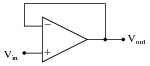
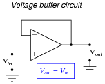
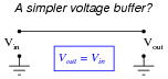
Question 10:
This operational amplifier circuit is often referred to as a voltage buffer, because it has unity gain (0 dB) and therefore simply reproduces, or "buffers," the input voltage:
|
|
What possible use is a circuit such as this, which offers no voltage gain or any other form of signal modification? Wouldn't a straight piece of wire do the same thing? Explain your answers.
|
|
Notes:
I have found that some students have difficulty with the terms "heavy" and "light" in reference to load characteristics. That a "heavy" load would have very few ohms of impedance, and a "light" load would have many ohms of impedance seems counter-intuitive to some. It all makes sense, though, once students realize the terms "heavy" and "light" refer to the amount of current drawn by the respective loads.
Ask your students to explain why the straight piece of wire fails to "buffer" the voltage signal in the same way the the opamp follower circuit does.
Question 11:
For all practical purposes, how much voltage exists between the inverting and noninverting input terminals of an op-amp in a functioning negative-feedback circuit?
Notes:
Ask your students to explain why there will be (practically) no voltage between the input terminals of an operational amplifier when it is used in a negative feedback circuit.
Question 12:
Just as certain assumptions are often made for bipolar transistors in order to simplify their analysis in circuits (an ideal BJT has negligible base current, IC = IE, constant b, etc.), we often make assumptions about operational amplifiers so we may more easily analyze their behavior in closed-loop circuits. Identify some of these ideal opamp assumptions as they relate to the following parameters:
- �
- Magnitude of input terminal currents:
- �
- Input impedance:
- �
- Output impedance:
- �
- Input voltage range:
- �
- Output voltage range:
- �
- Differential voltage (between input terminals) with negative feedback:
- �
- Magnitude of input terminal currents: infinitesimal
- �
- Input impedance: infinite
- �
- Output impedance: infinitesimal
- �
- Input voltage range: never exceeding +V/-V
- �
- Output voltage range: never exceeding +V/-V
- �
- Differential voltage (between input terminals) with negative feedback: infinitesimal
Notes:
Just in case your students are unfamiliar with the words infinite and infinitesimal, tell them they simply mean "bigger than big" and ßmaller than small", respectively.
Question 13:
The purpose of this circuit is to provide a pushbutton-adjustable voltage. Pressing one button causes the output voltage to increase, while pressing the other button causes the output voltage to decrease. When neither button is pressed, the voltage remains stable:
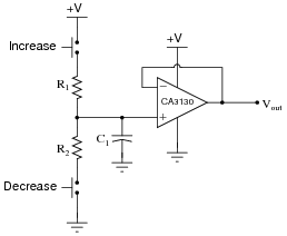
|
|
After working just fine for quite a long while, the circuit suddenly fails: now it only outputs zero volts DC all the time.
An experienced technician first checks the power supply voltage to see if it is within normal limits, and it is. Then, the technician checks the voltage across the capacitor. Explain why this is a good test point to check, and what the results of that check would tell the technician about the nature of the fault.
Challenge question: why do you suppose I specify a CA3130 operational amplifier for this particular circuit? What is special about this opamp that qualifies it for the task?
Notes:
Knowing where to check for critical signals in a circuit is an important skill, because it usually means the difference between efficiently locating a fault and wasting time. Ask your students to explain in detail the rationale behind checking for voltage across the capacitor, and (again, in detail) what certain voltage measurements at that point would prove about the nature of the fault.
Question 14:
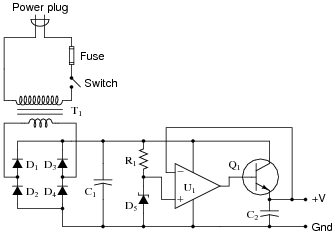
A student builds the following regulated AC-DC power supply circuit, but is dissatisfied with its performance:
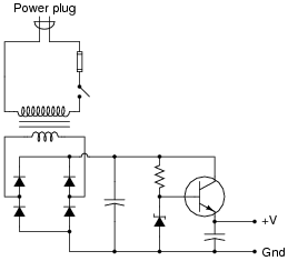
|
|
The voltage regulation is not as good as the student hoped. When loaded, the output voltage ßags" more than the student wants. When the zener diode's voltage is measured under the same conditions (unloaded output, versus loaded output), its voltage is noted to sag a bit as well. The student realizes that part of the problem here is loading of the zener diode through the transistor. In an effort to improve the voltage regulation of this circuit, the student inserts an opamp "voltage follower" circuit between the zener diode and the transistor:
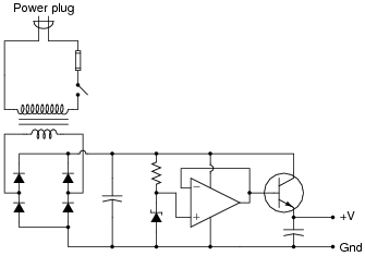
|
|
Now the zener diode is effectively isolated from the loading effects of the transistor, and by extension from the output load as well. The opamp simply takes the zener's voltage and reproduces it at the transistor base, delivering as much current to the transistor as necessary without imposing any additional load on the zener diode.
This modification does indeed improve the circuit's ability to hold a steady output voltage under changing load conditions, but there is still room for improvement. Another student looks at the modified circuit, and suggests one small change that dramatically improves the voltage regulation:
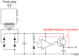
|
|
Now the output voltage holds steady at the zener diode's voltage with almost no ßag" under load! The second student is pleased with the success, but the first student does not understand why this version of the circuit functions any better than previous version. How would you explain this circuit's improved performance to the first student? How is an understanding of negative feedback essential to being able to comprehend the operation of this circuit?
Follow-up question: the new, improved circuit certainly exhibits better voltage regulation, but it also introduces something that the first student finds surprising: now the output voltage is approximately 0.7 volts greater than it used to be. Explain why.
Notes:
This is one of my favorite questions to ask students as they begin to learn how negative feedback works. It is an excellent "litmus test" for comprehension of negative feedback: those students who understand how and why negative feedback works will immediately grasp the significance of the modified feedback connection; those who do not understand negative feedback will fail to grasp why this circuit works at all. Spend as much time as you need discussing this circuit, because it holds the key to student understanding of a great many opamp circuits!
Question 15:
Predict how the operation of this regulated power supply circuit will be affected as a result of the following faults. Consider each fault independently (i.e. one at a time, no multiple faults):
|
|
- �
- Transformer T1 primary winding fails open:
- �
- Rectifying diode D3 fails open:
- �
- Rectifying diode D4 fails shorted:
- �
- Resistor R1 fails open:
- �
- Zener diode D5 fails open:
- �
- Operational amplifier U1 fails with output saturated positive:
- �
- Transistor Q1 fails open (collector-to-emitter):
For each of these conditions, explain why the resulting effects will occur.
- �
- Transformer T1 primary winding fails open: Output voltage falls to zero after filter capacitors C1 and C2 discharge.
- �
- Rectifying diode D3 fails open: No effect seen at no load, regulation falters sooner as load gets heavier.
- �
- Rectifying diode D4 fails shorted: Fuse may blow, diode D2 may fail due to overheating (and quickly blow the fuse if it also fails shorted).
- �
- Resistor R1 fails open: Output voltage falls to zero after filter capacitor C2 discharges.
- �
- Zener diode D5 fails open: Output voltage rises to nearly full (unregulated) value.
- �
- Operational amplifier U1 fails with output saturated positive: Output voltage rises to nearly full (unregulated) value.
- �
- Transistor Q1 fails open (collector-to-emitter): Output voltage falls to zero after filter capacitor C2 discharges.
Notes:
The purpose of this question is to approach the domain of circuit troubleshooting from a perspective of knowing what the fault is, rather than only knowing what the symptoms are. Although this is not necessarily a realistic perspective, it helps students build the foundational knowledge necessary to diagnose a faulted circuit from empirical data. Questions such as this should be followed (eventually) by other questions asking students to identify likely faults based on measurements.
Question 16:
This regulated power supply circuit has a problem. Instead of outputting 15 volts DC (exactly) as it should, it is outputting 0 volts DC to the load:
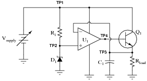
|
|
You measure 0.25 volts DC between TP4 and ground, and 20 volts between TP1 and ground, using your voltmeter. From this information, determine at least two independent faults that could cause this particular problem.
- �
- Opamp (U1) failed with output saturated negative.
- �
- Zener diode (D1) failed shorted.
- �
- Resistor R1 failed open.
Notes:
Ask your students to explain their reasoning, as to why they chose the component faults that they did. Also, ask them to identify any components they think are working properly (beyond a doubt).
Question 17:
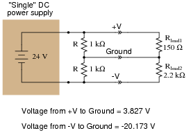
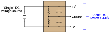
"Split" or "dual" DC power supplies are essential for powering many types of electronic circuits, especially certain types of operational amplifier circuits. If only a ßingle" DC power supply is not available, a ßplit" power supply may be roughly simulated through the use of a resistive voltage divider:
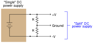
|
|
The problem with doing this is loading: if more current is drawn from one of the power supply rails than from the other, the ßplit" of voltage will become uneven. The only way that +V and -V will have the same (absolute) voltage value at the load is if the load impedance is balanced evenly between those rails and ground. This scenario is unlikely. Take for instance this example:
|
|
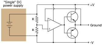
A simple opamp circuit, though, can correct this problem and maintain an even ßplit" of voltage between +V, Ground, and -V:
|
|
Explain how this circuit works. What function do the two resistors perform? How is negative feedback being used in this circuit?
Challenge question: if you plan on building this sort of circuit, placing a pair of bypass capacitors across the outputs is highly recommended. Explain why:
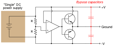
|
|
Notes:
This circuit is not only worthwhile to discuss with your students as an example of negative feedback in action, but it is also practical for them to use as an impromptu power supply ßplitter" when only a single supply is available. If you do decide to build this circuit, be careful of the transistors' power dissipations! Determine the maximum imbalance current to the load (how much current will be drawn through the Ground terminal), and then multiply that current by +V (or -V, absolute). This will be the maximum power dissipation value either transistor may have to safely handle.
In response to the challenge question, the wisdom of the bypass capacitors will be evident if a pulsating load (such as a brush-type DC motor) is placed between either "rail" and Ground. The opamp must swing its output back and forth very rapidly to turn on each transistor fast enough to counter dips in voltage caused by the pulsating load. Capacitors naturally resist change in voltage, and so are ideal for mitigating such voltage dips, easing the burden placed on the opamp.
Question 18:
Design a passive circuit that will create a ßplit" (+V/-V) power supply from a single voltage source:

|
|
|
|
Follow-up question: what design constraints will dictate the sizes of the resistors and capacitors?
Notes:
This simple filtered voltage divider circuit works well when the current draws are low, or at least very close to being equal, on the +V and -V load rails. It does not work so well for highly asymmetrical loads, or where low quiescent current draw is important (low-power battery circuits, for example). In applications requiring better +V/-V voltage stability, an opamp "follower" circuit is recommended after the voltage divider.
Question 19:
A complementary push-pull transistor amplifier built exactly as shown would perform rather poorly, exhibiting crossover distortion:
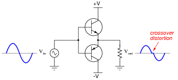
|
|
The simplest way to reduce or eliminate this distortion is by adding some bias voltage to each of the transistors' inputs, so there will never be a period of time when the two transistors are simultaneously cutoff:
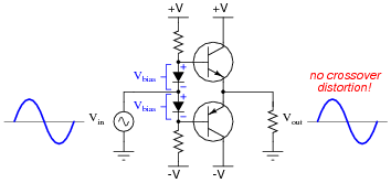
|
|
One problem with this solution is that just a little too much bias voltage will result in overheating of the transistors, as they simultaneously conduct current near the zero-crossing point of the AC signal. A more sophisticated method of mitigating crossover distortion is to use an opamp with negative feedback, like this:
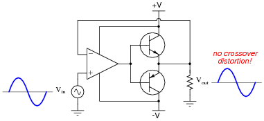
|
|
Explain how the opamp is able to eliminate crossover distortion in this push-pull amplifier circuit without the need for biasing.
Challenge question: a more practical design blends the two strategies like this:
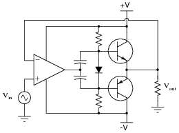
|
|
Explain why using less bias voltage and negative feedback with an opamp results in better performance than either method used alone.
Notes:
Much could be said about good amplifier circuit design in this question, but the fundamental point is for students to see how negative feedback coupled with the extremely high gain of the opamp minimizes crossover distortion. Be sure to focus students' attention on that point until they understand it well before launching into a discussion about the finer points of amplifier design.
It should be noted that this solution to crossover distortion in a push-pull amplifier circuit does not always yield the best results. In order for the opamp to ensure a smooth transition between half-cycles, its output must jump about 1.4 volts instantaneously to go from turning one transistor off to turning the other transistor on. Of course, no opamp can do this, because all have slew rate limitations. So, there will still be some crossover distortion, but not nearly as much as without the opamp (and with far less quiescent power dissipation that the two-diode solution!).
Question 20:
The parasitic capacitance naturally existing in two-wire cables can cause problems when connected to high-impedance electronic devices. Take for instance certain biomedical probes used to detect electrochemical events in living tissue. Such probes may be modeled as voltage sources in series with resistances, those resistances usually being rather large due to the probes' very small surface (contact) areas:
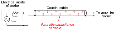
|
|
When connected to a cable with parasitic capacitance, a low-pass RC filter circuit is formed:
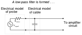
|
|
This low-pass filter (or passive integrator, if you wish) is purely unintentional. No one asked for it to be there, but it is there anyway just due to the natural resistance of the probe and the natural capacitance of the cable. Ideally, of course, we would like to be able to send the signal voltage (Vsignal) straight to the amplifier with no interference or filtering of any kind so we can see exactly what it is we're trying to measure.
One clever way of practically eliminating the effects of cable capacitance is to encase the signal wire in its own shield, and then drive that shield with the exact same amount of voltage from a voltage follower at the other end of the cable. This is called guarding:
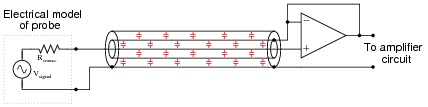
|
|
An equivalent schematic may make this technique more understandable:
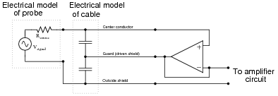
|
|
Explain why guarding the signal wire effectively eliminates the effects of the cable's capacitance. Certainly the capacitance is still present, so how can it not have any effect on the weak signal any more?
Follow-up question: although the center-to-guard capacitance may have zero volts across it at all times thanks to the opamp, the guard-to-(outer) shield capacitance still has the full signal voltage across it. Explain why this is of no concern to us, and why its presence does not form a low-pass filter as the original (unguarded) cable capacitance once did.
Notes:
Guarding is a technique used in many test and measurement scenarios, and it serves as a great example of opamps used as voltage followers.
If students are not convinced of the seriousness of cable capacitance in an application such as the one described, suggest these values to them and ask them to calculate the cutoff frequency of the low-pass filter formed by Rsignal and Ccable:
- �
- Rsignal = 20 MW
- �
- Ccable = 175 pF
Question 21:
Ideally, the input terminals of an operational amplifier conduct zero current, allowing us to simplify the analysis of many opamp circuits. However, in actuality there is a very small amount of current going through each of the input terminals of any opamp with BJT input circuitry. This may cause unexpected voltage errors in circuits.
Consider the following voltage buffer circuit:
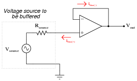
|
|
Ibias(-) does not cause any trouble for us, because it is completely supplied by the opamp's output. The other bias current, though, does cause trouble, because it must go through the source's Thévenin resistance. When it does, it drops some voltage across that intrinsic source resistance, skewing the amount of voltage actually seen at the noninverting terminal of the opamp.
A common solution to this is to add another resistor to the circuit, like this:
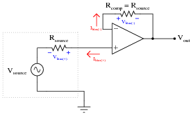
|
|
Explain why the addition of a resistor fixes the problem.
Notes:
A simple voltage buffer circuit is the easiest context in which to understand the function of a bias current compensating resistor, and so it is presented here to allow students to see its impact.