AC negative feedback opamp circuits
Question 1:
| Don't just sit there! Build something!! |
Learning to mathematically analyze circuits requires much study and practice. Typically, students practice by working through lots of sample problems and checking their answers against those provided by the textbook or the instructor. While this is good, there is a much better way.
You will learn much more by actually building and analyzing real circuits, letting your test equipment provide the änswers" instead of a book or another person. For successful circuit-building exercises, follow these steps:
- 1.
- Carefully measure and record all component values prior to circuit construction.
- 2.
- Draw the schematic diagram for the circuit to be analyzed.
- 3.
- Carefully build this circuit on a breadboard or other convenient medium.
- 4.
- Check the accuracy of the circuit's construction, following each wire to each connection point, and verifying these elements one-by-one on the diagram.
- 5.
- Mathematically analyze the circuit, solving for all voltage and current values.
- 6.
- Carefully measure all voltages and currents, to verify the accuracy of your analysis.
- 7.
- If there are any substantial errors (greater than a few percent), carefully check your circuit's construction against the diagram, then carefully re-calculate the values and re-measure.
Avoid using the model 741 op-amp, unless you want to challenge your circuit design skills. There are more versatile op-amp models commonly available for the beginner. I recommend the LM324 for DC and low-frequency AC circuits, and the TL082 for AC projects involving audio or higher frequencies.
As usual, avoid very high and very low resistor values, to avoid measurement errors caused by meter "loading". I recommend resistor values between 1 kW and 100 kW.
One way you can save time and reduce the possibility of error is to begin with a very simple circuit and incrementally add components to increase its complexity after each analysis, rather than building a whole new circuit for each practice problem. Another time-saving technique is to re-use the same components in a variety of different circuit configurations. This way, you won't have to measure any component's value more than once.
Notes:
It has been my experience that students require much practice with circuit analysis to become proficient. To this end, instructors usually provide their students with lots of practice problems to work through, and provide answers for students to check their work against. While this approach makes students proficient in circuit theory, it fails to fully educate them.
Students don't just need mathematical practice. They also need real, hands-on practice building circuits and using test equipment. So, I suggest the following alternative approach: students should build their own "practice problems" with real components, and try to mathematically predict the various voltage and current values. This way, the mathematical theory "comes alive," and students gain practical proficiency they wouldn't gain merely by solving equations.
Another reason for following this method of practice is to teach students scientific method: the process of testing a hypothesis (in this case, mathematical predictions) by performing a real experiment. Students will also develop real troubleshooting skills as they occasionally make circuit construction errors.
Spend a few moments of time with your class to review some of the "rules" for building circuits before they begin. Discuss these issues with your students in the same Socratic manner you would normally discuss the worksheet questions, rather than simply telling them what they should and should not do. I never cease to be amazed at how poorly students grasp instructions when presented in a typical lecture (instructor monologue) format!
A note to those instructors who may complain about the "wasted" time required to have students build real circuits instead of just mathematically analyzing theoretical circuits:
What is the purpose of students taking your course?
If your students will be working with real circuits, then they should learn on real circuits whenever possible. If your goal is to educate theoretical physicists, then stick with abstract analysis, by all means! But most of us plan for our students to do something in the real world with the education we give them. The "wasted" time spent building real circuits will pay huge dividends when it comes time for them to apply their knowledge to practical problems.
Furthermore, having students build their own practice problems teaches them how to perform primary research, thus empowering them to continue their electrical/electronics education autonomously.
In most sciences, realistic experiments are much more difficult and expensive to set up than electrical circuits. Nuclear physics, biology, geology, and chemistry professors would just love to be able to have their students apply advanced mathematics to real experiments posing no safety hazard and costing less than a textbook. They can't, but you can. Exploit the convenience inherent to your science, and get those students of yours practicing their math on lots of real circuits!
Question 2:
In a common-emitter transistor amplifier circuit, the presence of capacitance between the collector and base terminals - whether intrinsic to the transistor or externally connected - has the effect of turning the amplifier circuit into a low-pass filter, with voltage gain being inversely proportional to frequency:
|
|
Explain why this is. Why, exactly, does a capacitance placed in this location affect voltage gain? Hint: it has something to do with negative feedback!
Notes:
Students should realize that this is no hypothetical question. Intrinsic capacitance does indeed exist between the collector and base of a bipolar junction transistor (called the Miller capacitance), and this has a degenerating effect on voltage gain with increasing frequency. If time permits, you may wish to discuss how the common-collector and common-base amplifier configurations naturally avoid this problem.
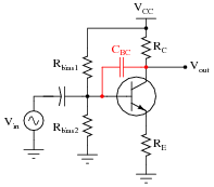
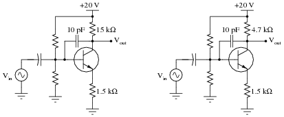
Question 3:
Which of the following amplifier circuits will be most affected by the base-collector capacitance (shown here as an externally-connected 10 pF capacitor) as frequency increases? Explain why.
|
|
Notes:
The purpose of this question is to get students to see, on a discrete component level, that for common-emitter amplifier there is a tradeoff between maximum gain and maximum operating frequency. This question foreshadows the concept of Gain-Bandwidth Product (GBW) in operational amplifier circuits.
Question 4:
A common problem encountered in the development of transistor amplifier circuits is unwanted oscillation resulting from parasitic capacitance and inductance forming a positive feedback loop from output to input. Often, these parasitic parameters are quite small (nanohenrys and picofarads), resulting in very high oscillation frequencies.
Another parasitic effect in transistor amplifier circuits is Miller-effect capacitance between the transistor terminals. For common-emitter circuits, the base-collector capacitance (CBC) is especially troublesome because it introduces a feedback path for AC signals to travel directly from the output (collector terminal) to the input (base terminal).
Does this parasitic base-to-collector capacitance encourage or discourage high-frequency oscillations in a common-emitter amplifier circuit? Explain your answer.
Notes:
Note that I chose to use a the word "mitigate" instead of give the answer in more plain English. Part of my reasoning here is to veil the given answer from immediate comprehension so that students must think a bit more. Another part of my reasoning is to force students' vocabularies to expand.
Question 5:
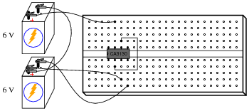
A student connects a model CA3130 operational amplifier as a voltage follower (or voltage buffer), which is the simplest type of negative feedback op-amp circuit possible:
|
|
With the noninverting input connected to ground (the midpoint in the split +6/-6 volt power supply), the student expects to measure 0 volts DC at the output of the op-amp. This is what the DC voltmeter registers, but when set to AC, it registers substantial AC voltage!
Now this is strange. How can a simple voltage buffer output alternating current when its input is grounded and the power supply is pure DC? Perplexed, the student asks the instructor for help. Öh," the instructor says, ÿou need a compensation capacitor between pins 1 and 8." What does the instructor mean by this cryptic suggestion?
Follow-up question: Are there any applications of an op-amp such as the CA3130 where a compensation capacitor is not needed, or worse yet would be an impediment to successful circuit operation? Hint: some models of op-amp (such as the model 741) have built-in compensation capacitors!
Notes:
Your students should have researched datasheets for the CA3130 op-amp in search of an answer to this question. Ask them what they found! Which terminals on the CA3130 op-amp do you connect the capacitor between? What size of capacitor is appropriate for this purpose?
Given the fact that some op-amp models come equipped with their own built-in compensation capacitor, what does this tell us about the CA3130's need for an external capacitor? Why didn't the manufacturer simply integrate a compensation capacitor into the CA3130's circuitry as they did with the 741? Or, to phrase the question more directly, ask your students to explain what disadvantage there is in connecting a compensation capacitor to an op-amp.
Question 6:
Some operational amplifiers come equipped with compensation capacitors built inside. The classic 741 design is one such opamp:

|
|
Find the compensation capacitor in this schematic diagram, and identify how it provides frequency-dependent negative feedback within the opamp to reduce gain at high frequencies.
Notes:
Answering this question will require a review of basic transistor amplifier theory, specifically different configurations of transistor amplifiers and their respective signal phase relationships.
Question 7:
Some operational amplifiers are internally compensated, while others are externally compensated. Explain the difference between the two. Hint: examples of each include the classic LM741 and LM101 operational amplifiers. Research their respective datasheets to see what you find on compensation!
Follow-up question: show how an external compensating capacitor may be connected to an opamp such as the LM101.
Notes:
Ask your students to explain why we might wish to use either type of opamp when building a circuit. In what applications do they think an internally-compensated opamp would be better, and in what applications do they think an externally-compensated opamp would be preferable?
Question 8:
Define "Gain-Bandwidth Product" (GBW) as the term applies to operational amplifiers.
Notes:
There are other means of defining Gain-Bandwidth Product, so do not be surprised if students present alternative definitions during the discussion time.
Question 9:
Define Ünity-Gain Bandwidth" (B1) as the term applies to operational amplifiers.
Notes:
It does not require a great deal of insight to recognize that unity-gain bandwidth (B1) and gain-bandwidth product (GBW) are pretty much the same thing. This would be a good point to bring up (in the form of a question!) for your students if you have already discussed GBW.
Question 10:
Explain the effect that compensation capacitance has on an operational amplifier's gain-bandwidth product (GBW). Does a larger compensation capacitance yield a greater GBW or a lesser GBW, and why?
Notes:
In this question, the really important aspect is not the answer given. What is important here is that students understand what GBW product is, and how it is affected by this thing we call "compensation capacitance" (another topic of research). The goal here is to get students to research these concepts and relate them together, so please do not be satisfied with any student answers that merely restate the answer given here! Ask students to explain what these terms and concepts mean, and to explain why the GBW product decreases with increased Ccomp.
Question 11:
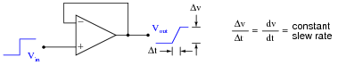
An important AC performance parameter for operational amplifiers is slew rate. Explain what ßlew rate" is, and what causes it to be less than optimal for an opamp.
Follow-up question: what would the output waveform of an opamp look like if it were trying to amplify a square wave signal with a frequency and amplitude exceeding the amplifier's slew rate?
Notes:
The follow-up question is very important, as it asks students to apply the concept of a maximum [dv/dt] to actual waveshapes. This is often discussed by introductory textbooks, though, so it should not be difficult for students to find good information to help them formulate an answer.
Question 12:
It strikes some students as odd that opamps would have a constant slew rate. That is, when subjected to a step-change input voltage, an opamp's output voltage would quickly ramp linearly over time, rather than ramp in some other way (such as the inverse exponential curve seen in RC and RL pulse circuits):
|
|
Yet, this effect has a definite cause, and it is found in the design of the opamp's internal circuitry: the voltage multiplication stages within operational amplifier circuits often use active loading for increased voltage gain. An example of active loading may be seen in the following schematic diagram for the classic 741 opamp, where transistor Q9 acts as an active load for transistor Q10, and where transistor Q13 provides an active load for transistor Q17:
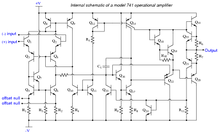
|
|
Explain how active loading creates the constant slew rate exhibited by operational amplifier circuits such as the 741. What factors account for the linear ramping of voltage over time?
|
Follow-up question: based on what you see here, determine what parameters could be changed within the internal circuitry of an operational amplifier to increase the slew rate.
Notes:
This question provides good review of fundamental capacitor behavior, and also explains why opamps have slew rates as they do.
Question 13:
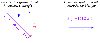
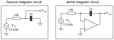
Calculate the impedance (in complex number form) ßeen" by the AC signal source as it drives the passive integrator circuit on the left, and the active integrator circuit on the right. In both cases, assume that nothing is connected to the Vout terminal:

|
|
|
|
Notes:
The most important thing to be learned here is that the opamp ïsolates" the signal source from whatever impedance is in the feedback loop, so that the input impedance (in this case, the 10 kW resistor) is the only impedance "visible" to that source. This has profound effects on the phase relationship between the output signal and the input signal.
Question 14:
Calculate the phase angle of the current drawn from the AC signal source as it drives the passive integrator circuit on the left, and the active integrator circuit on the right. In both cases, assume that nothing is connected to the Vout terminal:
|
|
Notes:
The most important thing to be learned here is that the opamp ïsolates" the signal source from whatever impedance is in the feedback loop, so that the input impedance (in this case, the 10 kW resistor) is the only impedance "visible" to that source. This has profound effects on the phase relationship between the output signal and the input signal.