Electrical conduction in semiconductors
Question 1:
In any electrically conductive substance, what are charge carriers? Identify the charge carriers in metallic substances, semiconducting substances, and conductive liquids.
- �
- Metals: "free" (conduction-band) electrons
- �
- Semiconductors: electrons and holes
- �
- Liquids: ions
Notes:
Metals are by far the simplest materials to understand with reference to electrical conduction. Point out to your students that it is this simplicity that makes metallic conduction so easy to mathematically model (Ohm's Law, E = I R).
Question 2:
A common conceptual model of electrons within atoms is the "planetary" model, with electrons depicted as orbiting satellites whirling around the "planet" of the nucleus. The physicist Ernest Rutherford is known as the inventor of this atomic model.
A major improvement over this conceptual model of the atom came from Niels Bohr, who introduced the idea that electrons inhabited ßtationary states" around the nucleus of an atom, and could only assume a new state by way of a quantum leap: a sudden "jump" from one energy level to another.
What led Bohr to his radical proposal of "quantum leaps" as an alternative to Rutherford's model? What experimental evidence led scientists to abandon the old planetary model of the atom, and how does this evidence relate to modern electronics?
Semiconductor electronics is made possible by the "quantum revolution" in physics. Electrical current travel through semiconductors is impossible to adequately explain apart from quantum theory.
Challenge question: think of an experiment that could be performed in the classroom to demonstrate the characteristic wavelengths emitted by ëxcited" atoms.
Notes:
It is no understatement to say that the advent of quantum theory changed the world, for it made possible modern solid-state electronics. While the subject of quantum theory can be arcane, certain aspects of it are nevertheless essential to understanding electrical conduction in semiconductors.
I cringe every time I read an introductory electronics textbook discuss electrons orbiting atomic nuclei like tiny satellites "held in orbit by electrostatic attraction and centrifugal force". Then, a few pages later, these books start talking about valence bands, conduction bands, forbidden zones, and a host of other phenomenon that make absolutely no sense within the planetary model of the atom, but only make sense in a quantum view (where electrons are only ällowed" to inhabit certain, discrete energy states around the nucleus).
In case none of your students are able to answer the challenge question, you may give them this hint: gas-discharge lamps (neon, hydrogen, mercury vapor, sodium, etc.)!
Question 3:
In solitary atoms, electrons are free to inhabit only certain, discrete energy states. However, in solid materials where there are many atoms in close proximity to each other, bands of energy states form. Explain what it means for there to be an energy "band" in a solid material, and why these "bands" form.
Notes:
Ask your students to think of analogies to illustrate this principle. Where else do we see multiple, individual entities joining together to form a larger (continuous) whole?
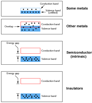
Question 4:
Engineers and scientists often use energy band diagrams to graphically illustrate the energy levels of electrons in different substances. Electrons are shown as solid dots:
|
|
Based on these diagrams, answer the following questions:
- �
- Which type of material is the best conductor of electricity, and why?
- �
- Which type of material is the worst conductor of electricity, and why?
- �
- Metals are the best conductors of electricity, because many of their electrons occupy the "conduction band" at normal temperatures.
- �
- Insulators are the worst conductors of electricity, because a tremendous amount of energy must be invested before an electron can "leap" across the large gap into the conduction band.
Notes:
I have given more information in the answer to this question than usual for me, because this subject is rather complex. One of the themes I'm trying to communicate in this question is that semiconductors are not just conductors with an unusually high amount of resistance. The mechanism of conduction in a pure semiconductor is fundamentally different from that of a metal.
Though this can become confusing, electrical conduction in metallic substances actually has two different forms: one where two electron bands overlap (permitting electrons to drift into the upper band and move between atoms), and one where the highest ünexcited" electron band is only partially filled (permitting electrons to drift into the upper regions of that same band and move between atoms). Whether or not this distinction is worthwhile to discuss in detail is a matter for you to decide.
Question 5:
Sadly, many introductory textbooks oversimplify the definition of a semiconductor by declaring them to be substances whose atoms contain four valence-shell (outer level) electrons. Silicon and germanium are traditionally given as the two major semiconductor materials used.
However, there is more to a ßemiconductor" than this simple definition. Take for instance the element carbon, which also has four valence electrons just like atoms of silicon and germanium. But not all forms of carbon are semiconducting: diamond is (at high temperatures), but graphite is not, and microscopic tubes known as "carbon nanotubes" may be made either conducting or semiconducting just by varying their diameter and "twist rate."
Provide a more accurate definition of what makes a ßemiconductor," based on electron bands. Also, name some other semiconducting substances.
- �
- Gallium arsenide (GaAs)
- �
- Gallium nitride
- �
- Silicon carbide
- �
- Some plastics (!)
While Gallium Arsenide is broadly used at the time of this writing (2004), the others are mostly in developmental stages. However, some of them show great promise, especially gallium nitride and silicon carbide in applications of high power, high temperature, and/or high frequency.
Notes:
I find it frustrating how many introductory electronics texts butcher the subject of semiconductor physics in an effort to "dumb it down" for technician consumption, when in fact these inaccuracies really obfuscate the subject. Furthermore, I have yet to read (October 2004) an introductory text that even bothers to mention substances other than silicon and germanium as semiconductors, despite a great deal of research and development taking place in the field of semiconductor materials
Thankfully, the internet provides a wealth of up-to-date information on the subject, much of it simple enough for beginning students to understand. This question is designed to get students researching sources other than their (poorly written) textbooks.
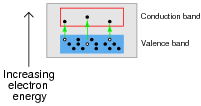
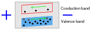
Question 6:
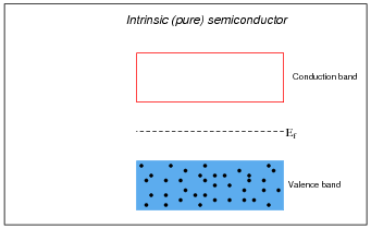
If a pure (ïntrinsic") semiconductor material is heated, the thermal energy liberates some valence-band electrons into the conduction band. The vacancies left behind in the valence band are called holes:
|
|
If an electrical voltage is applied across the heated semiconducting substance, with positive on the left and negative on the right, what will this do to the energy bands, and how will this affect both the electrons and the holes?
|
|
|
|
The presence of an electric field across the length of the material will cause the bands to slope, electrons moving toward the positive side and holes toward the negative.
Notes:
Holes are difficult concepts to grasp for some students. An analogy I find helpful for explaining how the absence of an electron may be though of as a particle is to refer to bubbles of air in water. When viewing bubbles of air in a clear, water-filled tube, it sure seems as though the bubbles are discrete particles, even though we know them to actually be voids where there is no water. And no one balks at the idea of assigning direction and speed to bubbles, even though they are really nothing rather than something!
The principle of energy bands sloping due to the presence of an electric field is vitally important for students to understand if they are to grasp the operation of a PN junction. An analogy that helps to visualize the electron and hole motion is to think of the two bands (conduction and valence) as two different pipes that can carry water. The upper pipe (the conduction band) is mostly empty, with only droplets of water running downhill. The bottom pipe (the valence band) is mostly full of water, with air bubbles running uphill.
One major point I wish to communicate here is that "hole flow" is not just a mirror-image of electron conduction. "Hole flow" is a fundamentally different mechanism of electron motion. Electrons are the only true charge carriers in any solid material, but "holes" are commonly referred to as "carriers" because they represent an easy-to-follow marker of valence electron motion. By referring to "holes" as entities unto themselves, it better distinguishes the two forms of electron motion (conduction-band versus valence-band).
Something you might want to point out to students, if they haven't already discovered it through their own research, is that there is no such thing as "hole flow" in metals. In metals, 100% of the conduction occurs through conduction-band electrons. This phenomenon of dual-mode electron flow only occurs when there is a band gap separating the valence and conduction bands. This is interesting to note, because many texts (even some high-level engineering textbooks!) refer to "conventional flow" current notation as "hole flow," even when the current exists in metal wires.
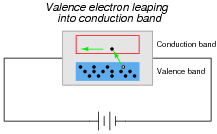
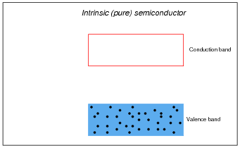
Question 7:
In perfectly pure (ïntrinsic") semiconductors, the only way charge carriers can exist is for valence electrons to "leap" into the conduction band with the application of sufficient energy, leaving a hole, or vacancy, behind in the valence band:
|
|
With sufficient thermal energy, these electron-hole pairs will form spontaneously. At room temperature, however, this activity is slight.
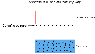
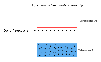
We may greatly enhance charge carrier formation by adding specific impurities to the semiconducting material. The energy states of atoms having different electron configurations do not precisely "blend" with the electron bands of the parent semiconductor crystal, causing additional energy levels to form.
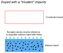
Some types of impurities will cause extra donor electrons to lurk just beneath the main conduction band of the crystal. These types of impurities are called pentavalent, because they have 5 valence electrons per atom rather than 4 as the parent substance typically possesses:
|
|
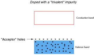
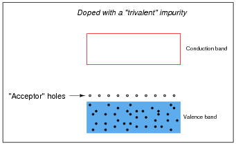
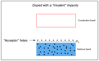
Other types of impurities will cause vacant electron levels (acceptor "holes") to form just above the main valence band of the crystal. These types of impurities are called trivalent, because they have 3 valence electrons per atom instead of 4:
|
|
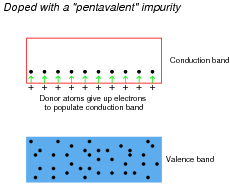
Compare the ease of forming free (conduction-band) electrons in a semiconductor material having lots of "donor" electrons, against that of an intrinsic (pure) semiconductor material. Which type of material will be more electrically conductive?
Likewise, compare the ease of forming valence-band holes in a semiconductor material having lots of äcceptor" holes, against that of an intrinsic (pure) semiconductor material. Which type of material will be more electrically conductive?
|
|
Likewise, trivalent äcceptor" atoms contribute to holes in the valence band:
|
|
In either case, the addition of impurities to an otherwise pure semiconductor material increases the number of available charge carriers.
Notes:
The most important concept for students to grasp here is that the addition of impurities increases the number of available charge carriers in a semiconducting substance. What was essentially an insulator in its pure state may be made conductive to varying degrees by adding impurities.
Question 8:
Describe the difference between an intrinsic and an extrinsic semiconducting substance.
Notes:
Just a simple definition here, nothing more. This is easily referenced in any introductory textbook.
Question 9:
What type of substance(s) must be added to an intrinsic semiconductor in order to produce "donor" electrons? When this is done, how do we denote this type of "doped" semiconducting substance?
Likewise, what type of substance(s) must be added to an intrinsic semiconductor in order to produce äcceptor" holes? When this is done, how to we denote this type of "doped" semiconducting substance?
To create acceptor holes, you must add a substance with a lesser number of valence electrons than the base semiconductor material. When this is done, it is called a P-type semiconductor.
Follow-up question: identify some common "donor" (N-type) and äcceptor" (P-type) dopants.
Notes:
When doping silicon and germanium substrates, the materials used are classified as either pentavalent or trivalent substances. Ask your students which one of these terms refers to the greater valence number, and which refers to the lesser valence number.
Question 10:
What effect does doping concentration have on the electrical conductivity of an extrinsic semiconductor?
Notes:
A couple of technical terms are used in this question (doping, extrinsic). Be sure to ask your students what they mean, if only for the sake of review. Also, ask your students to relate their answer in terms of charge carriers.
Question 11:
What must be done to an intrinsic semiconductor to turn it into an "N-type" semiconductor?
Notes:
Nothing much to comment on here, as this sort of question may be easily answered through research of any introductory textbook.
Question 12:
What must be done to an intrinsic semiconductor to turn it into a "P-type" semiconductor?
Notes:
Nothing much to comment on here, as this sort of question may be easily answered through research of any introductory textbook.
Question 13:
In extrinsic semiconductors, what are majority carriers and how do they differ from minority carriers?
Notes:
We speak of pure semiconductor materials, and of "doping" pieces of semiconductor material with just the right quantity and type(s) of dopants, but the reality is it is impossible to assure perfect quality control, and thus there will be other impurities in any semiconductor sample.
Ask your students to specifically identify the majority and minority charge carriers for "P" and "N" type extrinsic semiconductors. In each case, are they electrons, or holes?
Question 14:
What effect does temperature have on the electrical conductivity of a semiconducting material? How does this compare with the effect of temperature on the electrical conductivity of a typical metal?
Notes:
The answer to this question is a short review on temperature coefficients of resistance (a), for those students who may not recall the subject from their DC circuit studies. As always, though, the most important point of this question is why conductivity increases for semiconductors. Ask your students to relate their answer to the concept of charge carriers in semiconducting substances.
An interesting bit of trivia you could mention to your students is that glass - normally an excellent insulator of electricity - may be made electrically conductive by heating. Glass must be heated until it is red-hot before it becomes really conductive, so it is not an easy phenomenon to demonstrate. I found this gem of an experiment in an old book: Demonstration Experiments in Physics, first edition (fourth impression), copyright 1938, by Richard Manliffe Sutton, Ph.D.
Question 15:
Explain what the Fermi level is for a substance.
Notes:
It is sometimes helpful to use analogies for illustrative purposes. An analogy for Fermi level is to imagine a pot of boiling water, where water molecules represent electrons and height represents energy level. Under ambient temperature conditions, there are many water molecules (electrons) leaving the liquid surface, and some that are returning to it. Cool the pot below the boiling point, however, and all the water molecules return to the liquid where the uppermost level represents the Fermi level in a substance.
Question 16:
Draw the approximate locations of the Fermi levels in these three energy level diagrams:
|
|
|
|
|
|
|
|
|
|

|
|
Notes:
Note how much the Fermi level is affected by the addition of dopants to an otherwise pure semiconducting material. Understanding this effect is critical to the understanding of PN semiconductor junctions.
Question 17:
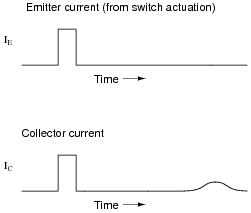
A fascinating experiment carried out by J. R. Hayes and W. Shockley in the early 1950's involved a bar of N-doped germanium with two metal point contacts labeled Ë" and "C," for Ëmitter" and "Collector," respectively:
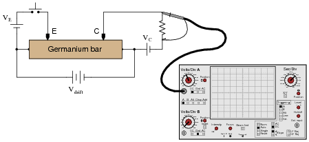
|
|
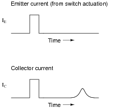
Upon actuating the switch, two distinct pulses were noted on the oscilloscope display:
|
|
With less drift voltage (Vdrift) applied across the length of the bar, the second pulse was seen to be further delayed and more diffused:
|
|
The instantaneous effect of the first pulse (precisely timed with the closure of the switch) is not the most interesting facet of this experiment. Rather, the second (delayed) pulse is. Explain what caused this second pulse, and why its shape depended on Vdrift.
Notes:
This tidbit of semiconductor history was found in Electronics for Scientists and Engineers, by R. Ralph Benedict, on pages 113 and 114. Like many other engineering textbooks of the 1950's and 1960's, this publication is at once a treasure trove of technical information and a model of clarity. I only wish the technician-level textbooks of today could be so lucid as the engineering-level textbooks of decades ago. As you might have guessed, I enjoy haunting used book stores in search of vintage engineering texts!