Regulated power sources
Question 1:
| Don't just sit there! Build something!! |
Learning to mathematically analyze circuits requires much study and practice. Typically, students practice by working through lots of sample problems and checking their answers against those provided by the textbook or the instructor. While this is good, there is a much better way.
You will learn much more by actually building and analyzing real circuits, letting your test equipment provide the änswers" instead of a book or another person. For successful circuit-building exercises, follow these steps:
- 1.
- Carefully measure and record all component values prior to circuit construction, choosing resistor values high enough to make damage to any active components unlikely.
- 2.
- Draw the schematic diagram for the circuit to be analyzed.
- 3.
- Carefully build this circuit on a breadboard or other convenient medium.
- 4.
- Check the accuracy of the circuit's construction, following each wire to each connection point, and verifying these elements one-by-one on the diagram.
- 5.
- Mathematically analyze the circuit, solving for all voltage and current values.
- 6.
- Carefully measure all voltages and currents, to verify the accuracy of your analysis.
- 7.
- If there are any substantial errors (greater than a few percent), carefully check your circuit's construction against the diagram, then carefully re-calculate the values and re-measure.
When students are first learning about semiconductor devices, and are most likely to damage them by making improper connections in their circuits, I recommend they experiment with large, high-wattage components (1N4001 rectifying diodes, TO-220 or TO-3 case power transistors, etc.), and using dry-cell battery power sources rather than a benchtop power supply. This decreases the likelihood of component damage.
As usual, avoid very high and very low resistor values, to avoid measurement errors caused by meter "loading" (on the high end) and to avoid transistor burnout (on the low end). I recommend resistors between 1 kW and 100 kW.
One way you can save time and reduce the possibility of error is to begin with a very simple circuit and incrementally add components to increase its complexity after each analysis, rather than building a whole new circuit for each practice problem. Another time-saving technique is to re-use the same components in a variety of different circuit configurations. This way, you won't have to measure any component's value more than once.
Notes:
It has been my experience that students require much practice with circuit analysis to become proficient. To this end, instructors usually provide their students with lots of practice problems to work through, and provide answers for students to check their work against. While this approach makes students proficient in circuit theory, it fails to fully educate them.
Students don't just need mathematical practice. They also need real, hands-on practice building circuits and using test equipment. So, I suggest the following alternative approach: students should build their own "practice problems" with real components, and try to mathematically predict the various voltage and current values. This way, the mathematical theory "comes alive," and students gain practical proficiency they wouldn't gain merely by solving equations.
Another reason for following this method of practice is to teach students scientific method: the process of testing a hypothesis (in this case, mathematical predictions) by performing a real experiment. Students will also develop real troubleshooting skills as they occasionally make circuit construction errors.
Spend a few moments of time with your class to review some of the "rules" for building circuits before they begin. Discuss these issues with your students in the same Socratic manner you would normally discuss the worksheet questions, rather than simply telling them what they should and should not do. I never cease to be amazed at how poorly students grasp instructions when presented in a typical lecture (instructor monologue) format!
A note to those instructors who may complain about the "wasted" time required to have students build real circuits instead of just mathematically analyzing theoretical circuits:
What is the purpose of students taking your course?
If your students will be working with real circuits, then they should learn on real circuits whenever possible. If your goal is to educate theoretical physicists, then stick with abstract analysis, by all means! But most of us plan for our students to do something in the real world with the education we give them. The "wasted" time spent building real circuits will pay huge dividends when it comes time for them to apply their knowledge to practical problems.
Furthermore, having students build their own practice problems teaches them how to perform primary research, thus empowering them to continue their electrical/electronics education autonomously.
In most sciences, realistic experiments are much more difficult and expensive to set up than electrical circuits. Nuclear physics, biology, geology, and chemistry professors would just love to be able to have their students apply advanced mathematics to real experiments posing no safety hazard and costing less than a textbook. They can't, but you can. Exploit the convenience inherent to your science, and get those students of yours practicing their math on lots of real circuits!
Question 2:
Complete the table of output voltages for several given values of input voltage in this common-collector amplifier circuit. Assume that the transistor is a standard silicon NPN unit, with a nominal base-emitter junction forward voltage of 0.7 volts:
|
|
-
Vin Vout
0.0 V
0.5 V
1.0 V
1.5 V
5.0 V
7.8 V
Based on the values you calculate, explain why the common-collector circuit configuration is often referred to as an emitter follower.
-
Vin Vout
0.0 V 0.0 V
0.5 V 0.0 V
1.0 V 0.3 V
1.5 V 0.8 V
5.0 V 4.3 V
7.8 V 7.1 V
The voltage at the transistor's emitter terminal approximately "follows" the voltage applied to the base terminal, hence the name.
Notes:
At first, the ëmitter follower" transistor circuit may seem pointless, since the output voltage practically equals the input voltage (especially for input voltages greatly exceeding 0.7 volts DC). "What possible good is a circuit like this?" some of your students may ask. The answer to this question, of course, has to do with currents in the circuit, and not necessarily voltages.
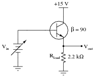
Question 3:
Complete the table of output voltages, output currents, and input currents for several given values of input voltage in this common-collector amplifier circuit. Assume that the transistor is a standard silicon NPN unit, with a nominal base-emitter junction forward voltage of 0.7 volts:
|
|
-
Vin Vout Iin Iout
0.0 V
0.4 V
1.2 V
3.4 V
7.1 V
10.8 V
Calculate the voltage and current gains of this circuit from the numerical values in the table:
|
|
-
Vin Vout Iin Iout
0.0 V 0.0 V 0.0 mA 0.0 mA
0.4 V 0.0 V 0.0 mA 0.0 mA
1.2 V 0.5 V 2.498 mA 0.227 mA
3.4 V 2.7 V 13.49 mA 1.227 mA
7.1 V 6.4 V 31.97 mA 2.909 mA
10.8 V 10.1 V 50.45 mA 4.591 mA
|
|
Notes:
The purpose of this question, besides providing practice for common-collector circuit DC analysis, is to show the current-amplification properties of the common-collector amplifier. This is an important feature, as there is no voltage amplification in this type of amplifier circuit.
This approach to determining transistor amplifier circuit voltage gain is one that does not require prior knowledge of amplifier configurations. In order to obtain the necessary data to calculate voltage gain, all one needs to know are the "first principles" of Ohm's Law, Kirchhoff's Laws, and basic operating principles of a bipolar junction transistor. This question is really just a thought experiment: exploring an unknown form of circuit by applying known rules of circuit components. If students doubt the efficacy of "thought experiments," one need only to reflect on the success of Albert Einstein, whose thought experiments as a patent clerk (without the aid of experimental equipment) allowed him to formulate the basis of his Theories of Relativity.
Question 4:
The purpose of a current mirror circuit is to maintain constant current through a load despite changes in that load's resistance:
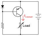
|
|
If we were to crudely model the transistor's behavior as an automatically-varied rheostat - constantly adjusting resistance as necessary to keep load current constant - how would you describe this rheostat's response to changes in load resistance?
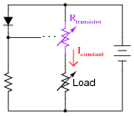
|
|
In other words, as Rload increases, what does Rtransistor do - increase resistance, decrease resistance, or remain the same resistance it was before? How does the changing value of Rtransistor affect total circuit resistance?
Notes:
This model of current mirror transistor behavior, albeit crude, serves as a good introduction to the subject of active loads in transistor amplifier circuits. This is where a transistor is configured to operate as a constant-current regulator, then placed in series with an amplifying transistor to yield much greater voltage gains than what is possible with a passive (fixed resistor) load.
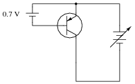
Question 5:
Based on what you know about bipolar junction transistors, what will the collector current do (increase, decrease, or remain the same) if the variable voltage source increases in voltage? The small, fixed voltage source (0.7 volts) is just enough to make the transistor conduct, but not enough to fully saturate it.
|
|
From the variable voltage source's perspective, what does the transistor circuit "look" like? It certainly does not look resistive, because a resistive circuit would increase current linearly with increases in applied voltage! If you could relate the behavior of this circuit to a common idealized electrical component, what would it be?
Notes:
This question is really nothing more than review of a transistor's characteristic curves. You might want to ask your students to relate this circuit's behavior to the common characteristic curves shown in textbooks for bipolar junction transistors. What portion of the characteristic curve is this transistor operating in while it regulates current?
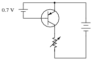
Question 6:
Based on what you know about bipolar junction transistors, what will the collector current do (increase, decrease, or remain the same) if the variable resistor's resistance is decreased? The small voltage source (0.7 volts) is just enough to make the transistor conduct, but not enough to fully saturate it.
|
|
From the variable resistor's perspective, what does the rest of the transistor circuit "look" like?
Notes:
This question is really nothing more than review of a transistor's characteristic curves. You might want to ask your students to relate this circuit's behavior to the common characteristic curves shown in textbooks for bipolar junction transistors. What portion of the characteristic curve is this transistor operating in while it regulates current?
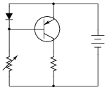
Question 7:
Describe what happens to the collector current of the transistor as the variable resistor's value is changed:
|
|
Hint: it is helpful to remember that the voltage drop across a PN junction is not exactly constant as the current through it varies. There is a nonlinear relationship between diode voltage drop (VD) and diode current (ID) as described by the diode equation:
|
Notes:
This circuit is really the beginning of a current mirror. I have found this to be an excellent starting point for student learning on linear transistor operation, as well as a good practical introduction of current regulation circuits. Once students recognize that bipolar transistors are essentially voltage-controlled current regulators (albeit very nonlinear!), they are ready to comprehend their application as signal amplifiers.
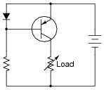
Question 8:
The circuit shown here is a simple current mirror. Explain what happens as the load resistance changes:
|
|
Most current mirrors are not built exactly like this. Instead of a diode, they use a transistor (identical to the other transistor) with the base and collector terminals shorted together:
|
|
Ideally, the two transistors are built on the same substrate material, so as to always be at equal temperature. Explain why this design is preferable to the first circuit (using the diode) shown in this question.
Follow-up question: explain how to adjust the regulated current's target value in either of these circuits.
Notes:
Current mirrors confuse beginning students primarily because they cannot be understood following the simplistic model of a silicon PN junction always dropping 0.7 volts. Rather, their operation is inextricably connected with Shockley's diode equation. This question is therefore not only a good review of that equation, but it also illustrates how the "models" we use to explain things are sometimes shown to be inadequate.
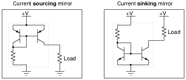
Question 9:
Two terms used commonly in electronics are sourcing and sinking, in reference to the direction of electric current between an active circuit and a load:
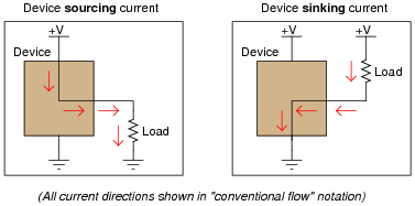
|
|
A practical example of where this distinction is important is in certain integrated circuits (IC "chips") where output pins may be able to only sink current, only source current, or both sink and source current.. Take a look at these two examples, each where an integrated circuit "chip" controls power to an LED. In one instance the IC is wired to source current to the LED, and in the other instance it is wired to sink current from the LED:
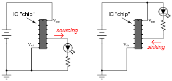
|
|
If an IC is only able to do one or the other (source or sink current, but not both), it makes a big difference how you connect load devices to it! What makes the difference between a circuit that is able to source current versus a circuit that is able to sink current is the internal configuration of its transistors.
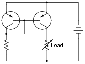
Similarly, a current mirror circuit may be built to either source current or sink current, but not do both. Draw current mirror circuits within the dotted-line boxes suitable for sourcing and sinking current to a load resistor:
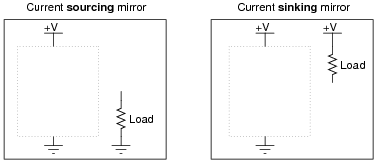
|
|
|
|
Notes:
This question challenges students' ability to "manipulate" the basic current mirror circuit into two different configurations. Depending on how well your students grasp the basic concept, you might want to spend extra discussion time comparing the two circuits, tracing current through each and discussing their operation in general.
Although it may seem trivial to an experienced instructor or electronics professional, variations of circuit designs consisting solely of inverting components are often quite confusing to students, especially those weak in spatial-relations skills. I encourage you to work with those students regularly to build this important visualization skill.
Question 10:
Calculate the approximate amount of current this current mirror circuit will try to maintain through Rload, assuming silicon transistors (0.7 volts forward base-emitter junction drop):
|
|
Follow-up question: what would have to be changed in this circuit to increase the amount of current through the load resistor without changing the power supply voltage?
Notes:
Ask your students to explain how they obtained the answer to this question, step by step.
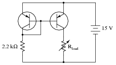
Question 11:
Calculate the approximate amount of current this current mirror circuit will try to maintain through Rload, assuming silicon transistors (0.7 volts forward base-emitter junction drop):
|
|
Also, calculate the approximate power dissipation of transistor Q2.
Notes:
Ask your students to explain how they obtained the answer to this question, step by step.
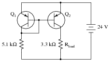
Question 12:
Calculate the approximate amount of current this current mirror circuit will try to maintain through Rload, assuming silicon transistors (0.7 volts forward base-emitter junction drop):
|
|
Also, calculate the approximate power dissipation of both transistors.
Follow-up question: what do the two power dissipation figures tell us about the relative power of two transistors handling the exact same currents? Explain why this is important in a current mirror circuit, and why it is customary to thermally bond Q1 and Q2 together in discrete-component current mirrors.
Notes:
Ask your students to explain how they obtained the answer to this question, step by step.
The follow-up question is an important one for a few reasons. First, students must be aware that transistor power dissipation is determined by more than just collector current. Secondly, the disparate dissipations of these two transistors will lead to inaccuracies in regulated current in a current mirror circuit if measures are not taken to equalize their temperatures.
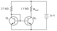
Question 13:
Choose a power supply voltage and resistance value for R1 that will maintain approximately 15 mA of current through the 1 kW load resistor. Assume the use of a silicon transistor:
|
|
To ensure plenty of regulation range (the ability to maintain regulated current over a wide range of load resistance values), design your circuit so that at least 20 volts VCE are dropped across transistor Q2. Also, calculate the approximate power dissipation of transistor Q2.
R1 = 2.287 kW Vsupply = 35 volts PQ2 � 300 mW
Notes:
Since there is more than one current answer for this design problem, be sure to ask students to present different solutions to it, asking them to explain how they obtained their answers to this question.
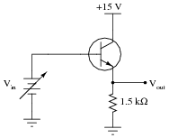
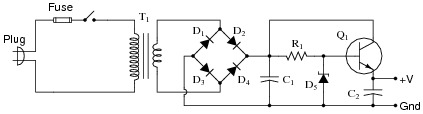
Question 14:
Describe the purpose of the transistor in this AC-DC power supply circuit:
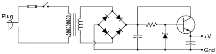
|
|
Notes:
Ask your students to identify the configuration of this transistor amplifier (common-base, common-emitter, or common collector?). After they have done this, ask them to identify the current gain of such an amplifier, given a transistor b value of 90.
Question 15:
Install a potentiometer in this circuit so that the regulated output voltage of this power supply becomes adjustable:
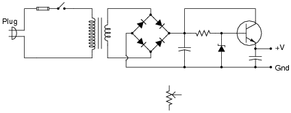
|
|
Challenge: leave the potentiometer symbol in its place, and make the necessary wire connections between it and the rest of the circuit!
|
|
Challenge question: for any given amount of load current, what voltage setting will cause the transistor to dissipate the most heat energy, low, medium, or high?
Notes:
Some students may choose to place the potentiometer on the output of the power supply (connecting to the transistor's emitter terminal). While this will work, technically, it is not a good solution because the load current will be severely limited by the potentiometer's resistance. Discuss with your students why the circuit drawn in the answer is more practical.
The answer to the challenge question is nonintuitive, but it makes sense once you determine what variables affect transistor power dissipation (emitter current, and VCE).
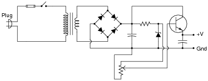
Question 16:
Calculate the approximate output voltage of this regulated power supply circuit and the amount of current through the zener diode under no-load conditions:
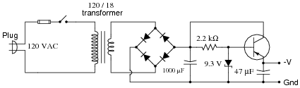
|
|
Notes:
Calculating the output voltage is a much simpler task than calculating the zener diode's current! Have your students explain their problem-solving techniques for this circuit.
Question 17:
Calculate the approximate output voltage of this regulated power supply circuit, the amount of current through the zener diode, and the (unregulated) voltage across the 1000 mF capacitor, all under no-load conditions:
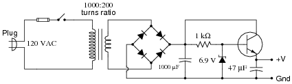
|
|
Notes:
Calculating the output voltage is a much simpler task than calculating the zener diode's current! Have your students explain their problem-solving techniques for this circuit.
Question 18:
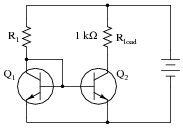
Predict how all component voltages and currents in this circuit will be affected as a result of the following faults. Consider each fault independently (i.e. one at a time, no multiple faults):
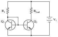
|
|
- �
- Resistor R1 fails open:
- �
- Transistor Q1 fails open, collector to emitter:
- �
- Transistor Q1 fails shorted, collector to emitter:
- �
- Transistor Q2 fails open, collector to emitter:
- �
- Transistor Q2 fails shorted, collector to emitter:
- �
- Load fails shorted:
For each of these conditions, explain why the resulting effects will occur.
- �
- Resistor R1 fails open: No current through Q1, no current through Q2, no current through load, no voltage dropped across Q1, full voltage dropped across collector-emitter of Q2.
- �
- Transistor Q1 fails open, collector to emitter: Approximately the same current through R1, increased current through Q2 base, increased current through Q2 collector (load current),and less voltage dropped between collector-emitter of Q2.
- �
- Transistor Q1 fails shorted, collector to emitter: Increased current through R1, almost zero current through all terminals of Q2 and the load, full voltage dropped across collector-emitter of Q2.
- �
- Transistor Q2 fails open, collector to emitter: No change in current for R1 or Q1, zero load current, full voltage dropped across collector-emitter of Q2.
- �
- Transistor Q2 fails shorted, collector to emitter: Current through R1 will most likely increase, zero voltage dropped across collector-emitter of Q2, increased current through Q2 and load.
- �
- Load fails shorted: No change in any current (in reality, load current will slightly increase), increased voltage drop across collector-emitter of Q2, possible overheating of Q2.
Notes:
The purpose of this question is to approach the domain of circuit troubleshooting from a perspective of knowing what the fault is, rather than only knowing what the symptoms are. Although this is not necessarily a realistic perspective, it helps students build the foundational knowledge necessary to diagnose a faulted circuit from empirical data. Questions such as this should be followed (eventually) by other questions asking students to identify likely faults based on measurements.
Question 19:
Predict how this power supply circuit's output voltage will be affected as a result of the following faults. Also note whether or not any other components in this circuit will become stressed as a result of each fault. Consider each fault independently (i.e. one at a time, no multiple faults):

|
|
- �
- Transformer T1 primary winding fails shorted:
- �
- Transformer T1 secondary winding fails open:
- �
- Rectifying diode D3 fails open:
- �
- Zener diode D5 fails open:
- �
- Zener diode D5 fails shorted:
- �
- Resistor R1 fails open:
- �
- Capacitor C2 fails shorted:
For each of these conditions, explain why the resulting effects will occur.
- �
- Transformer T1 primary winding fails shorted: Fuse immediately blows, then output voltage falls to zero (after filter capacitors have discharged).
- �
- Transformer T1 secondary winding fails open: Output voltage falls to zero (after filter capacitors C1 and C2 have discharged).
- �
- Rectifying diode D3 fails open: No change in output voltage (except when heavily loaded, where there will be increased ripple voltage).
- �
- Zener diode D5 fails open: Output voltage rises to approximately same level as unregulated voltage (across capacitor C1).
- �
- Zener diode D5 fails shorted: Output voltage falls to zero (as quickly as C2 can discharge), resistor R1 may overheat.
- �
- Resistor R1 fails open: Output voltage falls to zero (as quickly as C2 can discharge).
- �
- Capacitor C2 fails shorted: Output voltage falls to a very low value, transistor Q1 will most likely overheat.
Notes:
The purpose of this question is to approach the domain of circuit troubleshooting from a perspective of knowing what the fault is, rather than only knowing what the symptoms are. Although this is not necessarily a realistic perspective, it helps students build the foundational knowledge necessary to diagnose a faulted circuit from empirical data. Questions such as this should be followed (eventually) by other questions asking students to identify likely faults based on measurements.
Question 20:
Suppose this regulated power supply circuit used to function fine, but now has stopped outputting any DC voltage at all:
|
|
Initial diagnostic measurements show there to be full DC (unregulated) voltage across capacitor C1, and no DC voltage between the transistor base and ground. From this data, where would you suspect the problem is?
Notes:
Ask your students why the diagnostic measurements described in the question are good points to check (in the order that they were taken).
Question 21:
Many different types of sensors work on the principle of a variable resistance representing a different physical quantity. One such sensor is the common fuel level sensor used in automotive, marine, and industrial fuel storage applications:
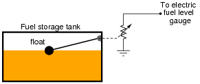
|
|
As the fuel level in the tank changes, the float position will change, changing the sensor's resistance. This resistance change is detected by an electric gauge (a special type of meter), which then provides visual indication of fuel level in the tank.
We must have some accurate way of measuring electrical resistance in order for this scheme to work. One common technique for doing this is to pass a constant current through the sensor resistance and then measure the voltage dropped across it. Since current mirror circuits function as current regulators, and therefore may be used as current sources if supplied with an external voltage, we could use a current mirror to force constant current through the fuel level sensor:
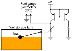
|
|
One problem with the circuit shown is that the sensor current will change as the supply voltage (+V) changes. This may be important to us, because the DC system voltage on an automobile may not be very stable, and this could lead to inaccuracies in fuel level measurement.
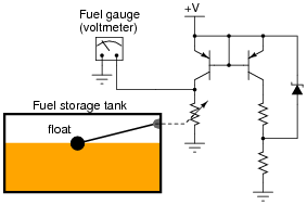
Figure out a way we could use a zener diode to stabilize the voltage in this current mirror circuit so that supply voltage changes would have minimal effect on the amount of current through the variable-resistance sensor.
|
|
Notes:
Students may try to implement a voltage regulation system for the entire circuit, sensor and everything, but this is unnecessary. Using a zener diode to regulate voltage for the right-hand portion of the current mirror circuit so that the right-hand transistor (acting as diode) receives constant current is all that is necessary. The left-hand transistor should faithfully regulate current through the sensor despite changes in sensor resistance and changes in supply voltage.
Question 22:
A very useful feature for a regulated voltage source is an electronic current limit: a circuit that limits the amount of current deliverable to a load, so as to avoid needless fuse-blowing. The combination of transistor Q2 and resistor R2 provides just this feature for the following voltage regulator circuit:
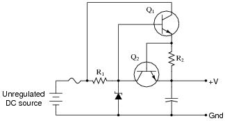
|
|
Describe how transistor Q2 limits the current sourced to a direct short-circuit across the load terminals.
Follow-up question: what component value(s) would we have to change in order to adjust the current limit in this power supply circuit?
Notes:
Ask your students to identify what it is that turns transistor Q2 on.
If students have difficulty understanding the limiting function of transistor Q2, just tell them to replace Q2 with a direct short (between the collector and emitter terminals of Q2), and re-analyze the circuit. They should see that transistor Q1 is unable to turn on in this condition.
A very helpful strategy in analyzing what happens in an electronic circuit as variables change is to imagine those variables assuming extreme states. In this case, to see the trend that occurs when Q2 starts to conduct, imagine Q2 conducting perfectly (a short between collector and emitter). Conversely, if we wanted to see what the circuit would do under conditions where Q2 is in cutoff mode, just replace Q2 with an open-circuit. While not always reliable, this technique often helps to overcome mental obstacles in analysis, and is a skill you should encourage in your students' discussion sessions often.
Question 23:
Suppose you had the boring job of manually maintaining the output voltage of a DC generator constant. Your one and only control over voltage is the setting of a rheostat:
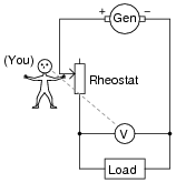
|
|
What would you have to do to maintain the load voltage constant if the load resistance changed so as to draw more current? Being that your only control over load voltage is the adjustment of a variable resistance in series with the generator, what does this imply about the generator's output voltage (directly across the generator terminals), compared to the target load voltage?
Note: this general voltage control scheme is known as series regulation, where a series resistance is varied to control voltage to a load.
Notes:
The direction of rheostat adjustment should be obvious, as is the fact that the generator's voltage must be at least as high as the intended (target) load voltage. However, it may not be obvious to all that the generator's voltage cannot merely be equal to the intended load voltage.
To illustrate the necessity of this, ask your students how the system would work if the generator's output voltage was exactly equal to the intended load voltage. Emphasize the fact that the generator is not perfect: it has its own internal resistance, the value of which cannot be changed by you. What position would the rheostat have to be in, under these conditions, in order to maintain target voltage at the load? Could the target voltage be maintained at all?
Question 24:
Suppose you had the boring job of manually maintaining the output voltage of a DC generator constant. Your one and only control over voltage is the setting of a rheostat:
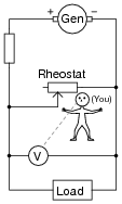
|
|
What would you have to do to maintain the load voltage constant if the load resistance changed so as to draw more current? Being that your only control over load voltage is the adjustment of a variable resistance in parallel with the load, what does this imply about the generator's output voltage (directly across the generator terminals), compared to the target load voltage?
Note: this general voltage control scheme is known as shunt regulation, where a parallel (shunt) resistance is varied to control voltage to a load.
Follow-up question: assuming the load voltage is maintained at a constant value by an astute rheostat operator despite fluctuations in load current, how would you characterize the current through the generator's windings? Does it increase with load current, decrease with load current, or remain the same? Why?
Notes:
The direction of rheostat adjustment should be obvious, as is the fact that the generator's voltage must be at least as high as the intended (target) load voltage. However, it may not be obvious to all that the generator's voltage cannot merely be equal to the intended load voltage.
To illustrate the necessity of this, ask your students how the system would work if the generator's output voltage was exactly equal to the intended load voltage. Emphasize the fact that the generator is not perfect: it has its own internal resistance, the value of which cannot be changed by you. What position would the rheostat have to be in, under these conditions, in order to maintain target voltage at the load? Could the target voltage be maintained at all?
A helpful analogy for students is that of a car with an automatic transmission, with its speed being controlled by the brake pedal while the accelerator pedal is maintained at a constant position. This is not the most energy-efficient method of speed control, but it will work within certain limits!
Question 25:
Describe how a zener diode is able to maintain regulated (nearly constant) voltage across the load, despite changes in load current:
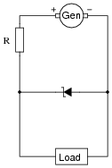
|
|
Follow-up question #1: if the generator happens to output some ripple voltage (as all electromechanical DC generators do), will any of that ripple voltage appear at the load, after passing through the zener diode voltage regulator circuit?
Follow-up question #2: would you classify the zener diode in this circuit as a series voltage regulator or a shunt voltage regulator? Explain your answer.
Challenge question: at what point is the zener diode unable to regulate load voltage? Is there some critical load condition at which the diode ceases to regulate voltage?
Notes:
Ask your students to describe how energy-efficient they think this circuit is. Do they suspect it would be more suitable for low-current applications or high-current applications?
Question 26:
Calculate the power dissipated by the 5-volt zener diode for the following values of motor current (assume the battery voltage remains constant at 12 volts):
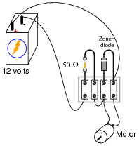
|
|
- �
- Imotor = 20 mA ; Pzener =
- �
- Imotor = 50 mA ; Pzener =
- �
- Imotor = 90 mA ; Pzener =
- �
- Imotor = 120 mA ; Pzener =
- �
- Imotor = 150 mA ; Pzener =
- �
- Imotor = 20 mA ; Pzener = 600 mW
- �
- Imotor = 50 mA ; Pzener = 450 mW
- �
- Imotor = 90 mA ; Pzener = 250 mW
- �
- Imotor = 120 mA ; Pzener = 100 mW
- �
- Imotor = 150 mA ; Pzener = 0 mW
Follow-up question: is load voltage maintained at 5 volts constant throughout this range of load currents (from 20 mA to 150 mA)?
Notes:
The follow-up question is fairly important here, as students need to realize the limitations of zener-based voltage regulators. Most importantly, are they able to calculate the exact current limit of a zener-based voltage regulator - the point at which it stops regulating?
It should be noted that the calculated answers shown here will not precisely match a real zener diode circuit, due to the fact that zener diodes tend to gradually taper off in current as the applied voltage nears the zener voltage rating rather than current sharply dropping to zero as a simpler model would predict.
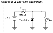
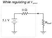
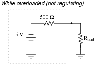
Question 27:
Is it possible to reduce this zener diode voltage regulator circuit to a Thévenin equivalent circuit? Explain why or why not.
|
|
|
|
|
|
Notes:
Some students may protest at the first Thévenin equivalent circuit (with a 0 ohm series resistance), because this would be a perfect voltage source. In reality, there would be a very small series resistance accounting for the slight voltage ßag" experienced under changing loads within the regulation range, but this is difficult to calculate.
Question 28:
Predict how all component voltages and currents in this circuit will be affected as a result of the following faults. Consider each fault independently (i.e. one at a time, no multiple faults):
|
|
- �
- Zener diode fails shorted:
- �
- Zener diode fails open:
- �
- Series resistor fails open:
- �
- Series resistor fails shorted:
For each of these conditions, explain why the resulting effects will occur.
- �
- Zener diode fails shorted: Little voltage across load, increased voltage across Rseries, increased current through source and Rseries.
- �
- Zener diode fails open: Increased voltage across load, decreased voltage across Rseries, decreased current through source and Rseries.
- �
- Series resistor fails open: No voltage across D1 or load, no current through D1 or load, no current through source.
- �
- Series resistor fails shorted: Full source voltage across load and D1, greatly increased current through D1, increased current through source, D1 will most likely overheat and fail.
Notes:
The purpose of this question is to approach the domain of circuit troubleshooting from a perspective of knowing what the fault is, rather than only knowing what the symptoms are. Although this is not necessarily a realistic perspective, it helps students build the foundational knowledge necessary to diagnose a faulted circuit from empirical data. Questions such as this should be followed (eventually) by other questions asking students to identify likely faults based on measurements.