Power conversion circuits
Question 1:
| Don't just sit there! Build something!! |
Learning to mathematically analyze circuits requires much study and practice. Typically, students practice by working through lots of sample problems and checking their answers against those provided by the textbook or the instructor. While this is good, there is a much better way.
You will learn much more by actually building and analyzing real circuits, letting your test equipment provide the änswers" instead of a book or another person. For successful circuit-building exercises, follow these steps:
- 1.
- Carefully measure and record all component values prior to circuit construction, choosing resistor values high enough to make damage to any active components unlikely.
- 2.
- Draw the schematic diagram for the circuit to be analyzed.
- 3.
- Carefully build this circuit on a breadboard or other convenient medium.
- 4.
- Check the accuracy of the circuit's construction, following each wire to each connection point, and verifying these elements one-by-one on the diagram.
- 5.
- Mathematically analyze the circuit, solving for all voltage and current values.
- 6.
- Carefully measure all voltages and currents, to verify the accuracy of your analysis.
- 7.
- If there are any substantial errors (greater than a few percent), carefully check your circuit's construction against the diagram, then carefully re-calculate the values and re-measure.
When students are first learning about semiconductor devices, and are most likely to damage them by making improper connections in their circuits, I recommend they experiment with large, high-wattage components (1N4001 rectifying diodes, TO-220 or TO-3 case power transistors, etc.), and using dry-cell battery power sources rather than a benchtop power supply. This decreases the likelihood of component damage.
As usual, avoid very high and very low resistor values, to avoid measurement errors caused by meter "loading" (on the high end) and to avoid transistor burnout (on the low end). I recommend resistors between 1 kW and 100 kW.
One way you can save time and reduce the possibility of error is to begin with a very simple circuit and incrementally add components to increase its complexity after each analysis, rather than building a whole new circuit for each practice problem. Another time-saving technique is to re-use the same components in a variety of different circuit configurations. This way, you won't have to measure any component's value more than once.
Notes:
It has been my experience that students require much practice with circuit analysis to become proficient. To this end, instructors usually provide their students with lots of practice problems to work through, and provide answers for students to check their work against. While this approach makes students proficient in circuit theory, it fails to fully educate them.
Students don't just need mathematical practice. They also need real, hands-on practice building circuits and using test equipment. So, I suggest the following alternative approach: students should build their own "practice problems" with real components, and try to mathematically predict the various voltage and current values. This way, the mathematical theory "comes alive," and students gain practical proficiency they wouldn't gain merely by solving equations.
Another reason for following this method of practice is to teach students scientific method: the process of testing a hypothesis (in this case, mathematical predictions) by performing a real experiment. Students will also develop real troubleshooting skills as they occasionally make circuit construction errors.
Spend a few moments of time with your class to review some of the "rules" for building circuits before they begin. Discuss these issues with your students in the same Socratic manner you would normally discuss the worksheet questions, rather than simply telling them what they should and should not do. I never cease to be amazed at how poorly students grasp instructions when presented in a typical lecture (instructor monologue) format!
A note to those instructors who may complain about the "wasted" time required to have students build real circuits instead of just mathematically analyzing theoretical circuits:
What is the purpose of students taking your course?
If your students will be working with real circuits, then they should learn on real circuits whenever possible. If your goal is to educate theoretical physicists, then stick with abstract analysis, by all means! But most of us plan for our students to do something in the real world with the education we give them. The "wasted" time spent building real circuits will pay huge dividends when it comes time for them to apply their knowledge to practical problems.
Furthermore, having students build their own practice problems teaches them how to perform primary research, thus empowering them to continue their electrical/electronics education autonomously.
In most sciences, realistic experiments are much more difficult and expensive to set up than electrical circuits. Nuclear physics, biology, geology, and chemistry professors would just love to be able to have their students apply advanced mathematics to real experiments posing no safety hazard and costing less than a textbook. They can't, but you can. Exploit the convenience inherent to your science, and get those students of yours practicing their math on lots of real circuits!
Question 2:
Describe what a dynamotor is, and what its purpose might be in an electrical system.
Notes:
The answer here is purposely vague, as I want students to research the details themselves.
Question 3:
What is a DC-DC converter circuit, and what applications might such a circuit be used for?
Notes:
In many cases, DC-DC converters find use in large systems that were not designed well (i.e. with proper DC voltages provided by a common AC-DC supply circuit). However, converter circuits do have more legitimate uses, including applications where isolation is required between two DC circuits. Ask your students what ëlectrical isolation" is any why it might be important.
Question 4:
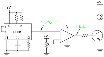
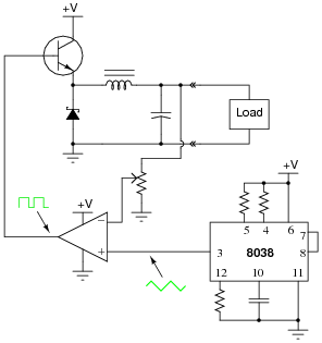
This circuit uses an 8038 waveform generator IC (integrated circuit) to produce a ßawtooth" waveform, which is then compared against a variable DC voltage from a potentiometer:
|
|
The result is a pulse waveform to the base of the power transistor, of the same frequency as the sawtooth waveform. Normally in circuits such as this, the frequency is at least several hundred Hertz.
Explain what happens to the brightness of the lamp when the potentiometer wiper is moved closer to +V, and when it is moved closer to ground.
Notes:
This question is a good review of comparator operation, and it introduces the concept of duty cycle, if your students have not encountered it before. Ask your students to explain how and why the duty cycle changes as the potentiometer wiper is moved. Ask them to explain why the lamp's brightness changes with duty cycle, and whether or not this is an efficient method of power control.
Question 5:
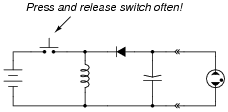
This circuit generates a pulse of DC voltage sufficient to energize the neon lamp, every time the switch is opened:
|
|
Describe the principle of operation for this simple circuit, and also how it could be modified to produce continuous high-voltage DC power.
Hint: how does a common AC-DC power supply circuit convert pulses of rectified DC into a relatively ßmooth" DC output?
|
|
Follow-up question: how would you recommend we äutomate" this circuit so that a person does not have to keep pressing and releasing the switch for it to generate a continuous DC output voltage?
Notes:
Ask your students to explain their solutions for äutomating" the switch's action. Prepare yourself for some creative answers!
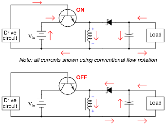
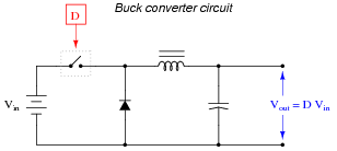
Question 6:
The schematic diagram shown here is for a "buck" converter circuit, a type of DC-DC ßwitching" power conversion circuit:
|
|
In this circuit, the transistor is either fully on or fully off; that is, driven between the extremes of saturation or cutoff. By avoiding the transistor's äctive" mode (where it would drop substantial voltage while conducting current), very low transistor power dissipations can be achieved. With little power wasted in the form of heat, ßwitching" power conversion circuits are typically very efficient.
Trace all current directions during both states of the transistor. Also, mark the inductor's voltage polarity during both states of the transistor.
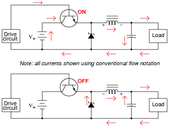
|
|
Follow-up question: how does the load voltage of this converter relate to the supply (battery) voltage? Does the load receive more or less voltage than that provided by the battery?
Challenge question: why do you suppose a Schottky diode is used in this circuit, as opposed to a regular (PN) rectifying diode?
Notes:
Ask your students why they think this circuit is called a buck converter. "Buck" usually refers to something that is in opposition. What is being opposed in this circuit?
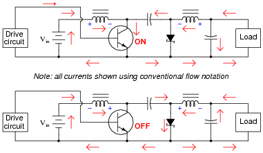
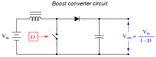
Question 7:
The schematic diagram shown here is for a "boost" converter circuit, a type of DC-DC ßwitching" power conversion circuit:
|
|
In this circuit, the transistor is either fully on or fully off; that is, driven between the extremes of saturation or cutoff. By avoiding the transistor's äctive" mode (where it would drop substantial voltage while conducting current), very low transistor power dissipations can be achieved. With little power wasted in the form of heat, ßwitching" power conversion circuits are typically very efficient.
Trace all current directions during both states of the transistor. Also, mark the inductor's voltage polarity during both states of the transistor.
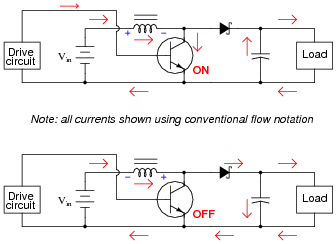
|
|
Follow-up question: how does the load voltage of this converter relate to the supply (battery) voltage? Does the load receive more or less voltage than that provided by the battery?
Challenge question: why do you suppose a Schottky diode is used in this circuit, as opposed to a regular (PN) rectifying diode?
Notes:
Ask your students why they think this circuit is called a boost converter. "Boost" usually refers to something that is aiding something else. What is being aided in this circuit?
Question 8:
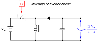
The schematic diagram shown here is for an ïnverting" converter circuit, a type of DC-DC ßwitching" power conversion circuit:
|
|
In this circuit, the transistor is either fully on or fully off; that is, driven between the extremes of saturation or cutoff. By avoiding the transistor's äctive" mode (where it would drop substantial voltage while conducting current), very low transistor power dissipations can be achieved. With little power wasted in the form of heat, ßwitching" power conversion circuits are typically very efficient.
Trace all current directions during both states of the transistor. Also, mark the inductor's voltage polarity during both states of the transistor.
|
|
Notes:
Ask your students why they think this circuit is called an inverting converter.
Although it may not be evident from viewing the circuit schematic, this converter circuit is capable of stepping voltage up or down, making it quite versatile.
Question 9:
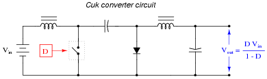
The schematic diagram shown here is for a "Cuk" converter circuit, a type of DC-DC ßwitching" power conversion circuit:
|
|
In this circuit, the transistor is either fully on or fully off; that is, driven between the extremes of saturation or cutoff. By avoiding the transistor's äctive" mode (where it would drop substantial voltage while conducting current), very low transistor power dissipations can be achieved. With little power wasted in the form of heat, ßwitching" power conversion circuits are typically very efficient.
Trace all current directions during both states of the transistor. Also, mark the both inductors' voltage polarities during both states of the transistor.
|
|
Follow-up question: how does the load voltage of this converter relate to the supply (battery) voltage? Does the load receive more or less voltage than that provided by the battery?
Notes:
The ßtrange" name of this circuit comes from the last name of the engineer who invented it! For more information, consult the writings of Rudy Severns on the general topic of switch-mode power conversion circuits.
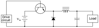
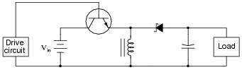
Question 10:
Predict how the operation of this buck converter circuit will be affected as a result of the following faults. Consider each fault independently (i.e. one at a time, no multiple faults):

|
|
- �
- Drive circuit fails with a constant "low" (0 volts) output signal:
- �
- Drive circuit fails with a constant "high" (+V) output signal:
- �
- Diode fails shorted:
- �
- Inductor fails open:
- �
- Capacitor fails shorted:
For each of these conditions, explain why the resulting effects will occur.
- �
- Drive circuit fails with a constant "low" (0 volts) output signal: Output voltage falls to zero after capacitor discharges.
- �
- Drive circuit fails with a constant "high" (+V) output signal: Output voltage rises to become approximately equal to Vin.
- �
- Diode fails shorted: Output voltage falls to zero, then transistor fails due to overheating.
- �
- Inductor fails open: Output voltage falls to zero after capacitor discharges.
- �
- Capacitor fails shorted: Output voltage falls to zero immediately.
Notes:
The purpose of this question is to approach the domain of circuit troubleshooting from a perspective of knowing what the fault is, rather than only knowing what the symptoms are. Although this is not necessarily a realistic perspective, it helps students build the foundational knowledge necessary to diagnose a faulted circuit from empirical data. Questions such as this should be followed (eventually) by other questions asking students to identify likely faults based on measurements.
Question 11:
Predict how the operation of this boost converter circuit will be affected as a result of the following faults. Consider each fault independently (i.e. one at a time, no multiple faults):

|
|
- �
- Drive circuit fails with a constant "low" (0 volts) output signal:
- �
- Drive circuit fails with a constant "high" (+V) output signal:
- �
- Diode fails shorted:
- �
- Inductor fails open:
- �
- Capacitor fails shorted:
For each of these conditions, explain why the resulting effects will occur.
- �
- Drive circuit fails with a constant "low" (0 volts) output signal: Output voltage rises to become approximately equal to Vin.
- �
- Drive circuit fails with a constant "high" (+V) output signal: Output voltage falls to zero after capacitor discharges.
- �
- Diode fails shorted: Output voltage exhibits very large "ripple" as the voltage repeatedly falls to zero and spikes back up each drive cycle, transistor may fail due to overheating.
- �
- Inductor fails open: Output voltage falls to zero after capacitor discharges.
- �
- Capacitor fails shorted: Output voltage falls to zero immediately.
Notes:
The purpose of this question is to approach the domain of circuit troubleshooting from a perspective of knowing what the fault is, rather than only knowing what the symptoms are. Although this is not necessarily a realistic perspective, it helps students build the foundational knowledge necessary to diagnose a faulted circuit from empirical data. Questions such as this should be followed (eventually) by other questions asking students to identify likely faults based on measurements.
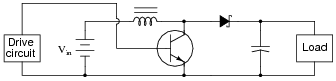
Question 12:
So-called linear regulator circuits work by adjusting either a series resistance or a shunt resistance to maintain output voltage at some fractional value of input voltage:
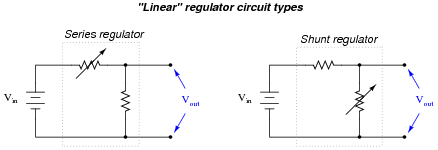
|
|
Typically, these variable resistances are provided by transistors rather than actual rheostats, which would have to be manually controlled.
Explain why a switching regulator circuit would perform the same task as a linear regulator circuit at a much greater efficiency. Also, identify which type(s) of switching regulator circuit would be best suited for the task of reducing an input voltage to a lesser output voltage.
Follow-up question: which type of linear regulator circuit does the traditional zener diode voltage regulator belong to, series or shunt?
Notes:
In the process of analyzing switching regulator functionality, it is easy for students to overlook the purpose for why they exist at all. Discuss the importance of power conversion efficiency, especially for electronic applications that are battery powered.
An important point to emphasize in this question is that most of the switching "regulator" circuits first shown to students are not actually regulators at all, but merely converters. A switching converter circuit does not become a regulator circuit until a feedback control is added. Such controls are usually too complex to introduce at the very beginning, so they are typically omitted for simplicity's sake. However, students should realize the difference between a switching regulator circuit and a mere switching converter circuit, lest they believe the converter to be capable of more than it is.
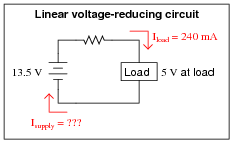
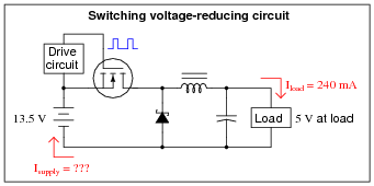
Question 13:
Shown here are two voltage-reducing circuits: both reducing a supply voltage of 13.5 volts down to 5 volts for a load.
|
|
|
|
Calculate the average supply current (Isupply) for both of these circuits. Assume that the switching circuit has negligible power losses in the transistor, inductor, capacitor, and diode. If the 13.5 volt source were an electrochemical battery, which battery would last longer powering the same load?
Follow-up question: calculate the power efficiency of the linear circuit, and comment on why it is so different from the switching circuit.
Notes:
Explain to your students that switching power conversion circuits are very efficient: typically 85 to 95 percent! It should be rather obvious which battery will last longer, and why. This is precisely why switching regulator circuits (DC-DC converters with a feedback network to stabilize output voltage) are used in place of linear regulator circuits (zener diode based) in many battery-powered electronic applications.
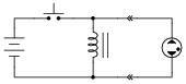
In essence, switching converter circuits act like DC transformers, able to step voltage down (or up), with current inversely proportional. Of course, the Law of Energy Conservation holds for switching circuits just as it does for transformers, and students may find this Law the easiest way to perform supply/load current calculations knowing the supply and load voltages:
|
|
If time permits, you might want to show your students a datasheet for a power converter controller, showing them how integrated circuits exist to precisely control the switching of MOSFETs for power converter circuits just like this.
Question 14:
The output voltage of a buck converter circuit is a function of the input voltage and the duty cycle of the switching signal, represented by the variable D (ranging in value from 0% to 100%), where D = [(ton)/(ton + toff)]:
|
|
Based on this mathematical relationship, calculate the output voltage of this converter circuit at these duty cycles, assuming an input voltage of 40 volts:
- �
- D = 0% ; Vout =
- �
- D = 25% ; Vout =
- �
- D = 50% ; Vout =
- �
- D = 75% ; Vout =
- �
- D = 100% ; Vout =
- �
- D = 0% ; Vout = 0 volts
- �
- D = 25% ; Vout = 10 volts
- �
- D = 50% ; Vout = 20 volts
- �
- D = 75% ; Vout = 30 volts
- �
- D = 100% ; Vout = 40 volts
Notes:
The calculations for this circuit should be very straightforward.
Note that the switching element in the schematic diagram is shown in generic form. It would never be a mechanical switch, but rather a transistor of some kind.
Question 15:
The output voltage of a boost converter circuit is a function of the input voltage and the duty cycle of the switching signal, represented by the variable D (ranging in value from 0% to 100%), where D = [(ton)/(ton + toff)]:
|
|
Based on this mathematical relationship, calculate the output voltage of this converter circuit at these duty cycles, assuming an input voltage of 40 volts:
- �
- D = 0% ; Vout =
- �
- D = 25% ; Vout =
- �
- D = 50% ; Vout =
- �
- D = 75% ; Vout =
- �
- D = 100% ; Vout =
- �
- D = 0% ; Vout = 40 volts
- �
- D = 25% ; Vout = 53.3 volts
- �
- D = 50% ; Vout = 80 volts
- �
- D = 75% ; Vout = 160 volts
- �
- D = 100% ; Vout = 0 volts
Notes:
The calculations for this circuit should be straightforward, except for the last calculation with a duty cycle of D = 100%. Here, students must take a close look at the circuit and not just follow the formula blindly.
Note that the switching element in the schematic diagram is shown in generic form. It would never be a mechanical switch, but rather a transistor of some kind.
Question 16:
The output voltage of an inverting converter circuit is a function of the input voltage and the duty cycle of the switching signal, represented by the variable D (ranging in value from 0% to 100%), where D = [(ton)/(ton + toff)]:
|
|
Based on this mathematical relationship, calculate the output voltage of this converter circuit at these duty cycles, assuming an input voltage of 40 volts:
- �
- D = 0% ; Vout =
- �
- D = 25% ; Vout =
- �
- D = 50% ; Vout =
- �
- D = 75% ; Vout =
- �
- D = 100% ; Vout =
- �
- D = 0% ; Vout = 0 volts
- �
- D = 25% ; Vout = 13.3 volts
- �
- D = 50% ; Vout = 40 volts
- �
- D = 75% ; Vout = 120 volts
- �
- D = 100% ; Vout = 0 volts
Notes:
The calculations for this circuit should be straightforward, except for the last calculation with a duty cycle of D = 100%. Here, students must take a close look at the circuit and not just follow the formula blindly.
Note that the switching element in the schematic diagram is shown in generic form. It would never be a mechanical switch, but rather a transistor of some kind.
Question 17:
The output voltage of a Cuk converter circuit (named after the engineer who invented it) is a function of the input voltage and the duty cycle of the switching signal, represented by the variable D (ranging in value from 0% to 100%), where D = [(ton)/(ton + toff)]:
|
|
Based on this mathematical relationship, calculate the output voltage of this converter circuit at these duty cycles, assuming an input voltage of 25 volts:
- �
- D = 0% ; Vout =
- �
- D = 25% ; Vout =
- �
- D = 50% ; Vout =
- �
- D = 75% ; Vout =
- �
- D = 100% ; Vout =
- �
- D = 0% ; Vout = 0 volts
- �
- D = 25% ; Vout = 8.33 volts
- �
- D = 50% ; Vout = 25 volts
- �
- D = 75% ; Vout = 75 volts
- �
- D = 100% ; Vout = 0 volts
Notes:
The calculations for this circuit should be straightforward, except for the last calculation with a duty cycle of D = 100%. Here, students must take a close look at the circuit and not just follow the formula blindly.
Note that the switching element in the schematic diagram is shown in generic form. It would never be a mechanical switch, but rather a transistor of some kind.
Astute students will note that there is no difference between the standard inverting converter circuit and the Cuk design, as far as output voltage calculations are concerned. This, however, does not mean the two circuits are equivalent in all ways! One definite advantage of the Cuk converter over the standard inverting converter is that the Cuk's input current never goes to zero during the switch's öff" cycle. This makes the Cuk circuit a "quieter" load as seen from the power source. Both inverting and buck converter circuits create a lot of electrical noise on the supply side if their inputs are unfiltered!
Question 18:
The following equations solve for the output voltage of various switching converter circuits (unloaded), given the switch duty cycle D and the input voltage:
|
|
|
Manipulate each of these equations to solve for duty cycle (D) in terms of the input voltage (Vin) and desired output voltage (Vout). Remember that duty cycle is always a quantity between 0 and 1, inclusive.
|
|
|
Notes:
Given the equations for these converter circuit types solving for output voltage in terms of input voltage and duty cycle D, this question is nothing more than an exercise in algebraic manipulation.
Note to your students that all of these equations assume a condition of zero load on the converter circuit. When loads are present, of course, the output voltage will not be the same as what is predicted by these neat, simple formulae. Although these DC-DC power converter circuits are commonly referred to as "regulators," it is somewhat misleading to do so because it falsely implies a capacity for self-correction of output voltage. Only when coupled to a feedback control network are any of these converter circuits capable of actually regulating output voltage to a set value.
Question 19:
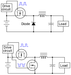
Many switching converter circuits use a switched MOSFET in place of a free-wheeling diode, like this:
|
|
The diode is a simple solution for providing the inductor a path for current when the main switching transistor is off. Why would anyone use another MOSFET in place of it, especially if this means the drive circuit has to become more complex (to drive two transistors at different times instead of just one transistor) to do the same task?
Notes:
It might not be obvious to some students why less voltage drop (across the MOSFET versus across the diode) has an impact on conversion efficiency. Remind them that power equals voltage times current, and that for any given current, a reduced voltage drop means reduced power dissipation. For the free-wheeling current path, less power dissipation means less power wasted, and less power that needs to be supplied by the source (for the same load power), hence greater efficiency.
Question 20:
A "boost" switching converter operating at 90% efficiency delivers 50 volts to a DC load. Calculate the load current if the input voltage is 17 volts and the input current is 9.3 amps.
Notes:
Calculations involving energy efficiency seem very confusing to some students. One principle that I often remind my students of is the Law of Energy Conservation, which prohibits any circuit from outputting more energy (or power) than it takes in. All too often, students mis-calculate in problems such as these, ending up with output powers greater than input powers!
Discuss problem-solving techniques, soliciting input from your students. Ideally, have individuals or groups present their techniques to the class as a whole, so you may observe their thinking processes and so that other students may learn how to become better problem-solvers.
Question 21:
A "buck" switching converter operating at 85% efficiency delivers 10 amps of current at 5 volts to a DC load. Calculate the input current if the input voltage is 23 volts.
Notes:
Calculations involving energy efficiency seem very confusing to some students. One principle that I often remind my students of is the Law of Energy Conservation, which prohibits any circuit from outputting more energy (or power) than it takes in. All too often, students mis-calculate in problems such as these, ending up with output powers greater than input powers!
Discuss problem-solving techniques, soliciting input from your students. Ideally, have individuals or groups present their techniques to the class as a whole, so you may observe their thinking processes and so that other students may learn how to become better problem-solvers.
Question 22:
A "boost" switching converter operating at 80% efficiency delivers 178 volts at 1 amp to a DC load. Calculate the input voltage if the input current is 11 amps.
Notes:
Calculations involving energy efficiency seem very confusing to some students. One principle that I often remind my students of is the Law of Energy Conservation, which prohibits any circuit from outputting more energy (or power) than it takes in. All too often, students mis-calculate in problems such as these, ending up with output powers greater than input powers!
Discuss problem-solving techniques, soliciting input from your students. Ideally, have individuals or groups present their techniques to the class as a whole, so you may observe their thinking processes and so that other students may learn how to become better problem-solvers.
Question 23:
The output voltage of a buck converter is a direct function of the switching transistor's duty cycle. Specifically, Vout = Vin([(ton)/(ttotal)]). Explain how the following PWM control circuit regulates the output voltage of the buck converter:
|
|
Follow-up question: what is the purpose of the potentiometer in this circuit?
Notes:
Here, students see a PWM control circuit coupled with a buck converter to provide voltage-regulated power conversion. Ask them what form of feedback (positive or negative?) is used in this circuit to regulate the output voltage at a steady value.
Let your students know that the PWM and feedback functions for switching regulator circuits are often provided in a single, application-specific integrated circuit rather than by a collection of discrete components and IC's as shown in the question.
Question 24:
The energy efficiency (h) of switching converter circuits typically remains fairly constant over a wide range of voltage conversion ratios. Describe how a switching regulator circuit (controlling load voltage to a pre-set value) äppears" to a power source of changing voltage if the regulator's load is constant. In other words, as the input voltage changes, what does the input current do?
Notes:
"Negative impedance" and "negative resistance" are phrases that may not be addressed very often in a basic electronics curriculum, but they have important consequences. If students experience difficulty understanding what the meaning of "negative" impedance is, remind them of this mathematical definition for impedance:
|
One of the unintended (and counter-intuitive) consequences of a circuit element with negative impedance can be oscillation, especially when the input power circuit happens to contain substantial inductance.
Question 25:
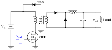
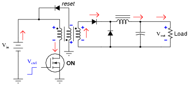
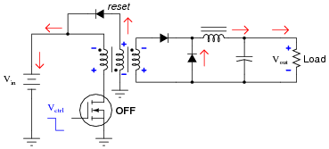
The following DC-DC converter circuit is called a forward converter. It is called this because the energy transfer from input to output occurs while the transistor is conducting, not while it is off. Verify this feature of the circuit by tracing current through all portions of it while the transistor is on:
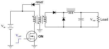
|
|
Now, trace current through the circuit while the transistor is off, and explain the purpose of the reset winding in the transformer:
|
|
|
|
|
|
The purpose of the reset winding is to rid the transformer core of stored energy during the off cycle. If this were not done, the transformer core's magnetic flux levels would reach saturation after just a few on/off cycles of the transistor.
Notes:
This question is a great review of the "dot convention" used in transformer schematic symbols.
Question 26:
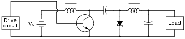
While simple "brute-force" AC-DC power supply circuits (transformer, rectifier, filter, regulator) are still used in a variety of electronic equipment, another form of power supply is more prevalent in systems where small size and efficiency are design requirements. This type of power supply is called a switching power supply.
Explain what a ßwitching power supply" is, and provide a schematic diagram of one for presentation and discussion. (Hint: most electronic computers use ßwitching" power supplies instead of "brute force" power supplies, so schematic diagrams should not be difficult to find.)
Notes:
While many ßwitching" power supply circuits will be too complex for beginning electronics students to fully understand, it will still be a useful exercise to analyze such a schematic and identify the major components (and functions).
Ask your students why ßwitching" power supplies are smaller and more efficient than "brute force" designs. Ask your students to note the type of transformer used in switching power supplies, and contrast its construction to that of line-frequency power transformers.
Question 27:
Suppose a friend of yours recently purchased an off-road vehicle. This friend also purchased a military-surplus spotlight, which he thinks would be a great accessory for off-road illumination at night. The only problem is, the spotlight is rated for 24 volts, while the electrical system in his vehicle is 12 volt.
Your friend asks you to engineer a solution for powering the 24-volt spotlight with the 12 volts available on his vehicle. Of course, you are not allowed to modify the vehicle's electrical system (change it to 24 volt generator, battery, starter motor, etc.), because it is new and still under warranty. What do you recommend to your friend?
Draw a component-level schematic diagram of your solution to this problem.
Notes:
Students may be inclined to give easy answers to this problem (üse a DC-DC converter!"), but the purpose of it is for students to explore solutions at the component level. Even if they do not yet understand how the circuitry works, they should be able to find complete solutions in their research, or at least enough schematics for sections of the conversion process for them to engineer a complete solution.
Remind your students that this is a powerful spotlight they're going to have to power! Their conversion system may have to handle hundreds of watts.
Question 28:
Describe the purpose and function of this circuit:
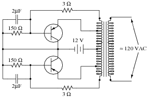
|
|
The 120 volt AC output provided by this circuit is definitely not sinusoidal, and the circuit's frequency varies with load. Can you think of any way(s) to improve these aspects of the circuit (you need not show details of your design modifications)?
Be prepared to explain what each of the transistors does, and how the transformer is able to function with DC power on its primary winding.
Notes:
This particular schematic was derived from a Triad brand transformer application, part number TY-75A. Recommended transistors were Delco 2N278, Bendix 2N678, Clevite 2N1146, and Delco 2N173. Slight variations in resistor and capacitor sizes may result in better performance. The 3 W resistors should have power ratings of at least 5 watts each, and the 150 W resistors should be rated for at least 20 watts each.
Question 29:
|
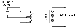
Electronic power conversion circuits known as inverters convert DC into AC by using transistor switching elements to periodically reverse the polarity of the DC voltage. Usually, inverters also increase the voltage level of the input power by applying the switched-DC voltage to the primary winding of a step-up transformer. You may think of an inverter's switching electronics as akin to double-pole, double-throw switch being flipped back and forth many times per second:
|
|
The first commercially available inverters produced simple square-wave output:
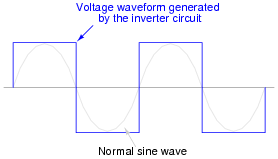
|
|
However, this caused problems for most power transformers designed to operate on sine-wave AC power. When powered by the square-wave output of such an inverter, most transformers would saturate due to excessive magnetic flux accumulating in the core at certain points of the waveform's cycle. To describe this in the simplest terms, a square wave possesses a greater volt-second product than a sine wave with the same peak amplitude and fundamental frequency.
This problem could be avoided by decreasing the peak voltage of the square wave, but then some types of powered equipment would experience difficulty due to insufficient (maximum) voltage:
|
|
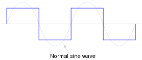
A workable solution to this dilemma turned out to be a modified duty cycle for the square wave:
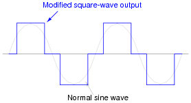
|
|
Calculate the fraction of the half-cycle for which this modified square wave is ön," in order to have the same volt-second product as a sine wave for one-half cycle (from 0 to p radians):
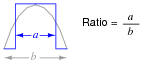
|
|
Hint: it is a matter of calculating the respective areas underneath each waveform in the half-cycle domain.
Challenge question: prove that the duty cycle fraction necessary for the square wave to have the same RMS value as the sine wave is exactly 1/2. Hint: the volts-squared-second product of the two waveforms must be equal for their RMS values to be equal!
Notes:
This problem is a great example of how integration is used in a very practical sense. Even if your students are unfamiliar with calculus, they should at least be able to grasp the concept of equal volt-second products for the two waveforms, and be able to relate that to the amount of magnetic flux accumulating in the transformer core throughout a cycle.
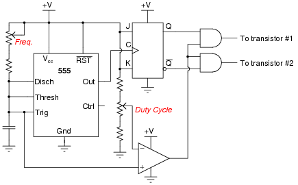
Question 30:
A common topology for DC-AC power converter circuits uses a pair of transistors to switch DC current through the center-tapped winding of a step-up transformer, like this:
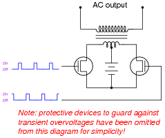
|
|
In order for this form of circuit to function properly, the transistor "firing" signals must be precisely synchronized to ensure the two are never turned on simultaneously. The following schematic diagram shows a circuit to generate the necessary signals:
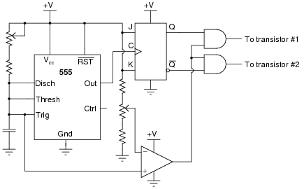
|
|
Explain how this circuit works, and identify the locations of the frequency control and pulse duty-cycle control potentiometers.
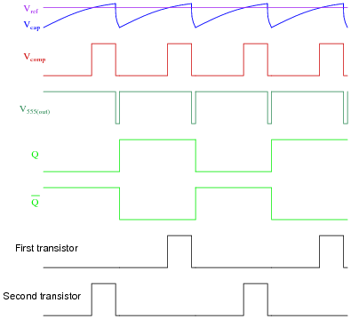
|
|
- �
- Vref = DC reference voltage set by duty cycle potentiometer
- �
- Vcap = Voltage measured at top terminal of the 555's capacitor
- �
- Vcomp = Comparator output voltage
- �
- V555(out) = 555 timer output voltage
- �
- Q = Noninverted output of J-K flip-flop
- �
- [`Q] = Inverted output of J-K flip-flop
|
|
Follow-up question: which direction would you have to move the frequency potentiometer to increase the output frequency of this circuit? Which direction would you have to move the duty cycle potentiometer to increase that as well?
Challenge question: suppose you were prototyping this circuit without the benefit of an oscilloscope. How could you test the circuit to ensure the final output pulses to the transistors are never simultaneously in the "high" logic state? Assume you had a parts assortment complete with light-emitting diodes and other passive components.
Notes:
This question is an exercise in schematic diagram and timing diagram interpretation. By the way, I have built and tested this circuit and I can say it works very well.