Timer circuits
Question 1:
| Don't just sit there! Build something!! |
Learning to analyze digital circuits requires much study and practice. Typically, students practice by working through lots of sample problems and checking their answers against those provided by the textbook or the instructor. While this is good, there is a much better way.
You will learn much more by actually building and analyzing real circuits, letting your test equipment provide the änswers" instead of a book or another person. For successful circuit-building exercises, follow these steps:
- 1.
- Draw the schematic diagram for the digital circuit to be analyzed.
- 2.
- Carefully build this circuit on a breadboard or other convenient medium.
- 3.
- Check the accuracy of the circuit's construction, following each wire to each connection point, and verifying these elements one-by-one on the diagram.
- 4.
- Analyze the circuit, determining all output logic states for given input conditions.
- 5.
- Carefully measure those logic states, to verify the accuracy of your analysis.
- 6.
- If there are any errors, carefully check your circuit's construction against the diagram, then carefully re-analyze the circuit and re-measure.
Always be sure that the power supply voltage levels are within specification for the logic circuits you plan to use. If TTL, the power supply must be a 5-volt regulated supply, adjusted to a value as close to 5.0 volts DC as possible.
One way you can save time and reduce the possibility of error is to begin with a very simple circuit and incrementally add components to increase its complexity after each analysis, rather than building a whole new circuit for each practice problem. Another time-saving technique is to re-use the same components in a variety of different circuit configurations. This way, you won't have to measure any component's value more than once.
Notes:
It has been my experience that students require much practice with circuit analysis to become proficient. To this end, instructors usually provide their students with lots of practice problems to work through, and provide answers for students to check their work against. While this approach makes students proficient in circuit theory, it fails to fully educate them.
Students don't just need mathematical practice. They also need real, hands-on practice building circuits and using test equipment. So, I suggest the following alternative approach: students should build their own "practice problems" with real components, and try to predict the various logic states. This way, the digital theory "comes alive," and students gain practical proficiency they wouldn't gain merely by solving Boolean equations or simplifying Karnaugh maps.
Another reason for following this method of practice is to teach students scientific method: the process of testing a hypothesis (in this case, logic state predictions) by performing a real experiment. Students will also develop real troubleshooting skills as they occasionally make circuit construction errors.
Spend a few moments of time with your class to review some of the "rules" for building circuits before they begin. Discuss these issues with your students in the same Socratic manner you would normally discuss the worksheet questions, rather than simply telling them what they should and should not do. I never cease to be amazed at how poorly students grasp instructions when presented in a typical lecture (instructor monologue) format!
I highly recommend CMOS logic circuitry for at-home experiments, where students may not have access to a 5-volt regulated power supply. Modern CMOS circuitry is far more rugged with regard to static discharge than the first CMOS circuits, so fears of students harming these devices by not having a "proper" laboratory set up at home are largely unfounded.
A note to those instructors who may complain about the "wasted" time required to have students build real circuits instead of just mathematically analyzing theoretical circuits:
What is the purpose of students taking your course?
If your students will be working with real circuits, then they should learn on real circuits whenever possible. If your goal is to educate theoretical physicists, then stick with abstract analysis, by all means! But most of us plan for our students to do something in the real world with the education we give them. The "wasted" time spent building real circuits will pay huge dividends when it comes time for them to apply their knowledge to practical problems.
Furthermore, having students build their own practice problems teaches them how to perform primary research, thus empowering them to continue their electrical/electronics education autonomously.
In most sciences, realistic experiments are much more difficult and expensive to set up than electrical circuits. Nuclear physics, biology, geology, and chemistry professors would just love to be able to have their students apply advanced mathematics to real experiments posing no safety hazard and costing less than a textbook. They can't, but you can. Exploit the convenience inherent to your science, and get those students of yours practicing their math on lots of real circuits!
Question 2:
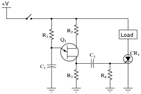
The following schematic diagram shows a timer circuit made from a UJT and an SCR:
|
|
Together, the combination of R1, C1, R2, R3, and Q1 form a relaxation oscillator, which outputs a square wave signal. Explain how a square wave oscillation is able to perform a simple time-delay for the load, where the load energizes a certain time after the toggle switch is closed. Also explain the purpose of the RC network formed by C2 and R4.
Follow-up question: how would you suggest we modify this circuit to make the time delay adjustable?
Notes:
Knowing that the UJT forms an oscillator, it is tempting to think that the load will turn on and off repeatedly. The first sentence in the answer explains why this will not happen, though.
I got the basic idea for this circuit from the second edition of Electronics for Industrial Electricians, by Stephen L. Herman.
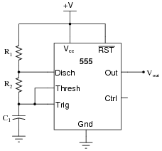
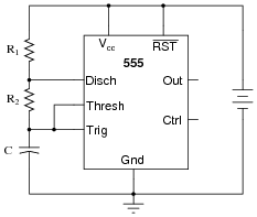
Question 3:
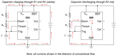
The model "555" integrated circuit is a very popular and useful "chip" used for timing purposes in electronic circuits. The basis for this circuit's timing function is a resistor-capacitor (RC) network:

|
|
In this configuration, the "555" chip acts as an oscillator: switching back and forth between "high" (full voltage) and "low" (no voltage) output states. The time duration of one of these states is set by the charging action of the capacitor, through both resistors (R1 and R2 in series). The other state's time duration is set by the capacitor discharging through one resistor (R2):
|
|
Obviously, the charging time constant must be tcharge = (R1 + R2)C, while the discharging time constant is tdischarge = R2C. In each of the states, the capacitor is either charging or discharging 50% of the way between its starting and final values (by virtue of how the 555 chip operates), so we know the expression e[(-t)/(t)] = 0.5, or 50 percent.f
Develop two equations for predicting the "charge" time and "discharge" time of this 555 timer circuit, so that anyone designing such a circuit for specific time delays will know what resistor and capacitor values to use.
Footnotes:
f For those who must know why, the 555 timer in this configuration is designed to keep the capacitor voltage cycling between 1/3 of the supply voltage and 2/3 of the supply voltage. So, when the capacitor is charging from 1/3VCC to its (final) value of full supply voltage (VCC), having this charge cycle interrupted at 2/3VCC by the 555 chip constitutes charging to the half-way point, since 2/3 of half-way between 1/3 and 1. When discharging, the capacitor starts at 2/3VCC and is interrupted at 1/3VCC, which again constitutes 50% of the way from where it started to where it was (ultimately) headed.
|
|
Notes:
Although it may seem premature to introduce the 555 timer chip when students are just finishing their study of DC, I wanted to provide a practical application of RC circuits, and also of algebra in generating useful equations. If you deem this question too advanced for your student group, by all means skip it.
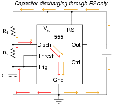
Incidentally, I simplified the diagram where I show the capacitor discharging: there is actually another current at work here. Since it wasn't relevant to the problem, I omitted it. However, some students may be adept enough to catch the omission, so I show it here:
|
|
Note that this second current (through the battery) does not go anywhere near the capacitor, and so is irrelevant to the discharge cycle time.
Question 4:
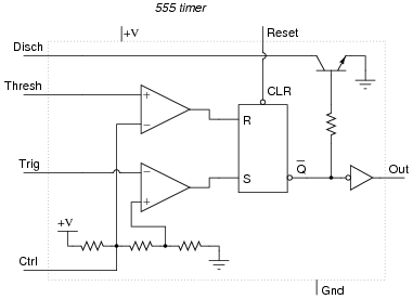
The type "555" integrated circuit is a highly versatile timer, used in a wide variety of electronic circuits for time-delay and oscillator functions. The heart of the 555 timer is a pair of comparators and an S-R latch:
|
|
The various inputs and outputs of this circuit are labeled in the above schematic as they often appear in datasheets ("Thresh" for threshold, "Ctrl" or "Cont" for control, etc.).
To use the 555 timer as an astable multivibrator, simply connect it to a capacitor, a pair of resistors, and a DC power source as such:
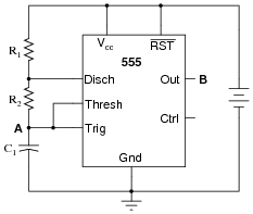
|
|
If were were to measure the voltage waveforms at test points A and B with a dual-trace oscilloscope, we would see the following:
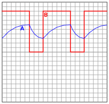
|
|
Explain what is happening in this astable circuit when the output is "high," and also when it is "low."
Follow-up question: algebraically manipulate the equation for this astable circuit's operating frequency, so as to solve for R2.
|
Challenge question: explain why the duty cycle of this circuit's output is always greater than 50%.
Notes:
This popular configuration of the 555 integrated circuit is well worth spending time analyzing and discussing with your students.
Question 5:
This astable 555 circuit has a potentiometer allowing for variable duty cycle:
|
|
With the diode in place, the output waveform's duty cycle may be adjusted to less than 50% if desired. Explain why the diode is necessary for that capability. Also, identify which way the potentiometer wiper must be moved to decrease the duty cycle.
To decrease the duty cycle, move the wiper up (toward the fixed resistor, away from the capacitor).
Challenge question: write an equation solving for the average current drawn by the 555 timer circuit as it charges and discharges the capacitor while generating a 50% duty cycle pulse. Assume that no current is drawn from the power supply by the circuit while the capacitor is discharging, and use this approximation of the capacitor Öhm's Law" equation for figuring average current through the charge cycle:
|
|
Notes:
This question really probes students' conceptual understanding of the 555 timer, used as an astable multivibrator (oscillator). If some students just can't seem to grasp the function of the diode, illuminate their understanding by having them trace the charging and discharging current paths. Once they understand which way current goes in both cycles of the timer, they should be able to recognize what the diode does and why it is necessary.
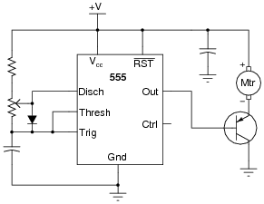
Question 6:
A popular use of the 555 timer is as a monostable multivibrator. In this mode, the 555 will output a pulse of fixed length when commanded by an input pulse:
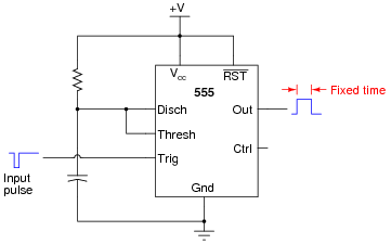
|
|
How low does the triggering voltage have to go in order to initiate the output pulse? Also, write an equation specifying the width of this pulse, in seconds, given values of R and C. Hint: the magnitude of the supply voltage is irrelevant, so long as it does not vary during the capacitor's charging cycle. Show your work in obtaining the equation, based on equations of RC time constants. Don't just copy the equation from a book or datasheet!
|
Notes:
Have your students show you how they mathematically derived their answer based on their knowledge of how capacitors charge and discharge. Many textbooks and datasheets provide this same equation, but it is important for students to be able to derive it themselves from what they already know of capacitors and RC time constants. Why is this important? Because in ten years they won't remember this specialized equation, but they will probably still remember the general time constant equation from all the time they spent learning it in their basic DC electricity courses (and applying it on the job). My motto is, "never remember what you can figure out."
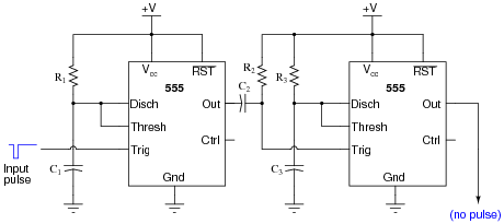
Question 7:
A sequential timer circuit may be constructed from multiple 555 timer ICs cascaded together. Examine this circuit and determine how it works:
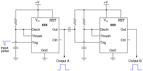
|
|
Can you think of any practical applications for a circuit such as this?
Follow-up question: when timer circuits are cascaded like this, do their time delays add or multiply to make the total delay time? Be sure to explain your reasoning.
Notes:
Practical applications abound for such a circuit. One whimsical application is to energize sequential tail-light bulbs for an automobile, to give an interesting turn-signal visual effect. A sequential timer circuit was used to do just this on certain years of (classic) Ford Cougar cars. Other, more utilitarian, applications for sequential timers include start-up sequences for a variety of electronic systems, traffic light controls, and automated household appliances.
Question 8:
Predict how the operation of this astable 555 timer circuit will be affected as a result of the following faults. Specifically, identify what will happen to the capacitor voltage (VC1) and the output voltage (Vout) for each fault condition. Consider each fault independently (i.e. one at a time, no multiple faults):
|
|
- �
- Resistor R1 fails open:
- �
- Solder bridge (short) across resistor R1:
- �
- Resistor R2 fails open:
- �
- Solder bridge (short) across resistor R2:
- �
- Capacitor C1 fails shorted:
For each of these conditions, explain why the resulting effects will occur.
- �
- Resistor R1 fails open: Capacitor voltage holds at last value, output voltage holds at last value.
- �
- Solder bridge (short) across resistor R1: Timer IC will become damaged at the first discharge cycle.
- �
- Resistor R2 fails open: Capacitor voltage holds at last value, output voltage holds at last value.
- �
- Solder bridge (short) across resistor R2: Oscillation frequency nearly doubles, and the duty cycle increases to nearly 100%.
- �
- Capacitor C1 fails shorted: Capacitor voltage goes to 0 volts DC, output voltage stays "high".
Notes:
The purpose of this question is to approach the domain of circuit troubleshooting from a perspective of knowing what the fault is, rather than only knowing what the symptoms are. Although this is not necessarily a realistic perspective, it helps students build the foundational knowledge necessary to diagnose a faulted circuit from empirical data. Questions such as this should be followed (eventually) by other questions asking students to identify likely faults based on measurements.
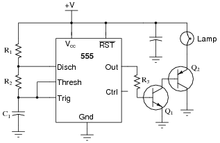
Question 9:
This circuit uses a "555" integrated circuit to produce a low-frequency square-wave voltage signal (seen between the Öut" terminal of the chip and ground), which is used to turn a pair of transistors on and off to flash a large lamp. Predict how this circuit will be affected as a result of the following faults. Consider each fault independently (i.e. one at a time, no multiple faults):
|
|
- �
- Transistor Q1 fails open (collector-to-emitter):
- �
- Transistor Q2 fails open (collector-to-emitter):
- �
- Resistor R3 fails open:
- �
- Transistor Q1 fails shorted (collector-to-emitter):
For each of these conditions, explain why the resulting effects will occur.
- �
- Transistor Q1 fails open (collector-to-emitter): Lamp remains off, no current through any terminal of Q2.
- �
- Transistor Q2 fails open (collector-to-emitter): Lamp remains off, no current through any terminal of Q2, normal base current through Q1, no current through collector of Q1.
- �
- Resistor R3 fails open: Lamp remains off, no current through any terminal of Q1 or Q2.
- �
- Transistor Q1 fails shorted (collector-to-emitter): Lamp remains on, full ön" current levels through terminals of Q1 and Q2.
Notes:
The purpose of this question is to approach the domain of circuit troubleshooting from a perspective of knowing what the fault is, rather than only knowing what the symptoms are. Although this is not necessarily a realistic perspective, it helps students build the foundational knowledge necessary to diagnose a faulted circuit from empirical data. Questions such as this should be followed (eventually) by other questions asking students to identify likely faults based on measurements.
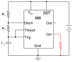
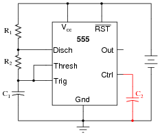
Question 10:
What would happen to the operation of this astable 555 timer circuit if a resistor were accidently connected between the "Control" terminal and ground? Explain the reason for your answer.
|
|
Follow-up question: does the addition of this resistor affect the output signal (pin 3) amplitude as well? Explain why or why not. If it amplitude is affected, does it increase or decrease with the resistor in place?
Notes:
Ask your students to explain why frequency and amplitude changes in this circuit. It is far too easy for a student to simply repeat the answer given by the worksheet! Hold your students accountable to reasoning through the operation of a circuit like this.
Question 11:
A student builds their first astable 555 timer circuit, using a TLC555CP chip. Unfortunately, it seems to have a problem. Sometimes, the output of the timer simply stops oscillating, with no apparent cause. Stranger yet, the problem often occurs at the precise time anyone moves their hand within a few inches of the circuit board (without actually touching anything!).
What could the student have done wrong in assembling this circuit to cause such a problem? What steps would you take to troubleshoot this problem?
Notes:
Every year it seems I have at least one student who experiences this particular problem, usually as a result of hasty circuit assembly (not making all necessary connections to pins on the chip). This is a good question to brainstorm with your class on, exploring possible causes and methods of diagnosis.
Question 12:
Identify at least one component fault that would cause the final 555 timer output to always remain low:
|
|
For each of your proposed faults, explain why it will cause the described problem.
- �
- Resistor R1 failed open.
- �
- Solder bridge past resistor R2.
- �
- No power to either 555 timer IC.
Notes:
Be sure to discuss the reasons why each of your students' proposed component faults would cause the final output to never go high. The possibilities range from the obvious to the obscure, and exploring them will strengthen your students' understanding of the 555 as a monostable multivibrator.
Question 13:
Pulse Width Modulation, or PWM, is a very popular means of controlling power to an electrical load such as a light bulb or a DC motor. With PWM control, the duty cycle of a high-frequency digital (on/off) signal is varied, with the effect of varying power dissipation at the load:
|
|
One of the major advantages to using PWM to proportion power to a load is that the final switching transistor operates with minimal heat dissipation. If we were to use a transistor in its linear (äctive") mode, it would dissipate far more heat when controlling the speed of this motor! By dissipating less heat, the circuit wastes less power.
Explain why the power transistor in this circuit runs cooler when buffering the PWM signal from the 555 timer, rather than if it were operated in linear mode. Also, identify which direction the potentiometer wiper must be moved to increase the speed of the motor.
Challenge question: suppose we needed to control the power of a DC motor, when the motor's operating voltage was far in excess of the 555 timer's operating voltage. Obviously, we need a separate power supply for the motor, but how would we safely interface the 555's output with the power transistor to control the motor speed? Draw a schematic diagram to accompany your answer.
To increase the speed of the motor, move the potentiometer wiper up (as pictured in the schematic).
Here is one possible solution to the problem of interfacing a 555 timer to a high-voltage DC motor:
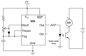
|
|
Notes:
There is much literature available discussing PWM power control, and its advantages over linear power control. Your students should have no difficulty finding it on their own!
Discuss with them the proposed solution to the high-voltage motor problem. What purpose(s) do/does the solid-state relay serve? Is there a way to achieve PWM control over the motor without using an optocoupled device? If so, how? Let your students show their solutions and discuss the practicality of each.
Question 14:
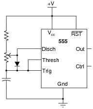
It is common to see a capacitor connected between the "Control" terminal and ground in 555 timer circuits, especially when precise timing is important.
|
|
Explain what purpose the capacitor C2 serves in this circuit.
Challenge question: what operational parameters of the circuit define the necessary capacitance value of C2?
Notes:
Decoupling power supply pins on a chip is important, but here students get to see another variation of decoupling. If time permits, work through a sample problem with your students sizing capacitor C2, given a certain operating frequency of the astable circuit. Note: this will give you another opportunity to use Thévenin's Theorem . . .
Question 15:
Special integrated circuits called delay elements or delay gates are manufactured to provide nanoseconds' worth of intentional time delays in digital circuits. Identify a part number for such an IC, research its datasheet, and describe an application where one might be needed.
Notes:
Discuss with your students why such devices exist, in light of the existence of 555 timers. Why couldn't a 555 timer be used for the same purpose as the 74LS31?
Question 16:
An important measurement of pulse waveforms is duty cycle. Give a precise. mathematical definition for this term.
Also, write an equation solving for pulse width given duty cycle (D) and frequency (f).
|
I'll let you figure out how to write an equation solving for pulse width (ton) in terms of duty cycle and frequency.
Notes:
Duty cycle is a very important concept, as analog information may be conveyed through the variable duty cycle of an otherwise digital pulse waveform. Discuss this application with your students, if time permits.
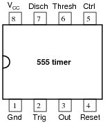
Question 17:
Research the "pinout" for a 555 timer integrated circuit, in an 8-pin DIP package. Then, label the pins as shown on this figure:
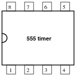
|
|
Question 18:
Write equations for the charging and discharging times of the capacitor, given the values of R1, R2, and C in a circuit of this design:
|
|
Base your equations on the general rules of RC time constant circuits. Don't just copy the completed equations from some reference book! Assume that the 555's discharge transistor is a perfect switch when turned on (0 volts drop). Note that the supply voltage is irrelevant to these calculations, so long as it remains constant during the charging cycle.
|
|
Follow-up questions: write an equation for the circuit's frequency, given values of R1, R2, and C. Then, write another equation for the circuit's duty cycle.
Notes:
Have your students show you how they mathematically derived their answer based on their knowledge of how capacitors charge and discharge. Many textbooks and datasheets provide this same equation, but it is important for students to be able to derive it themselves from what they already know of capacitors and RC time constants. Why is this important? Because in ten years they won't remember these specialized equations, but they will probably still remember the general time constant equation from all the time they spent learning it in their basic DC electricity courses (and applying it on the job). My motto is, "never remember what you can figure out."
The challenge questions are worthwhile to do in class, even if few students were able to derive them on their own. If nothing else, such an exercise reviews the meaning of "frequency" and its relationship with period, as well as the definition of "duty cycle."